Second Solid-State Imaging Forum open for registration

July 15th, 2014

Hello everyone,

All organizational and logistics details are settled, so I can open the registration for the second Solid-State Imaging Forum.  All information of the forum is shown on the website : www.harvestimaging.com/forum.php

Please notice, like last year, I will limit the number of seats to maximum 24.  This will enhance the learning experience.  Only in the case that we get substantially more registrants than this upper limit of 24, a second session can/will be considered.  If you are interested to attend, early registration is recommended for two reasons :

1) for you : to make sure you get a seat (first come, first serve),

2) for me : to get as early as possible an idea whether a second session is needed or not.  (A scond session  can not be organized just a few weeks before the event will take place,)

Thanks, and looking forward to see you at the forum,

Albert.

15-07-2014.

How to Measure Modulation Transfer Function (5)

July 4th, 2014

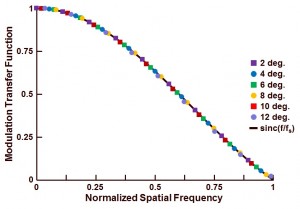
In the last blog the MTF measurement based on the slanted edge was introduced.  As mentioned in that blog, to understand all ins and outs of the method, it is very beneficial to develop a small, simple model of the sensor with a slanted edge projected on it.  And next, analyze the obtained, synthesized image.  This simulation tool is also used here to check out the sensitivity of the technique w.r.t. the angle of the slanted edge.

The result is shown in Figure 1.

Figure 1 : Effect of the slanted edge angle on the accuracy of the evaluation technique to characterize the MTF.

Shown are the MTF results obtained for a simulation of the angle being equal to 2 deg., 4 deg., 6 deg., 8 deg., 10 deg. and 12 deg.  The ideal curve, obtained by the calculation of the sinc-function, is included as well.  As can be seen from the curve :

  • All evaluations based on an angle between 2 deg. and 10 deg. seem to fit very well to the ideal curve,
  • The simulation result for an angle of 12 deg. shows some minor deviations from the ideal curve.

As a message from this simulation : angles of the slanted edge between 2 deg. and 10 deg. are very well suited for the MTF analysis.  Once the angle is larger than 10 deg., the slanted edge method starts loosing its accuracy.  The simulation results obtained here are fully in line with the advice of the ISO standard, which suggests also to use an angle of the slanted edge between 2 deg. and 10 deg.

Next time : how to implement oversampling and how to avoid aliasing effects during the measurements.

Albert, 04-07-2014.

How to Measure Modulation Transfer Function (4)

June 18th, 2014

The MTF or Modulation Transfer Function can be measured in various ways.  In the previous MTF-blogs the measurement by means of a Siemens Star testchart was discussed.  This method has particular advantages, but also has some limitations, mentioned in earlier blogs.  Another evaluation technique to characterize the MTF is based on the so-called slanted-edge method.  Explained in words, this method sounds very complicated, but in reality it is really pretty simple.

There are several good references describing the slanted-edge method, e.g. :

  • M. Estribeau and P. Magnan., in SPIE Proceedings, Vol. 5251, Sept. 2003,
  • T. Dutton et al. in SPIE Proceedings, Vol. 4486, 2002, pp. 219-246,
  • P.B. Burns, in Proceedings IS&T, 2000, pp 135-138,
  • S.E. Reichenback et al. In Optical Engineering, pp. 170-177, 1991.

This slanted edge method became an ISO standard, namely ISO 12233.  This is one of the very few ISO standards for image sensor and/or camera measurements.

The technique of the slanted edge can be described as follows :

  1. Image a vertically oriented edge (or a horizontal one for the MTF measurement in the other direction) onto the detector.  The vertical edge needs to be slightly tilted with respect to the columns of the sensor.  The exact tilting is of no importance, it is advisable to have a tilt of minimum 2o and maximum 10o w.r.t. the column direction.  A tilt within these limits gives the best and most reliable results for the MTF characterization.
  2. Each row of the detector gives a different Edge Spread Function (ESF), and the Spatial Frequency Response (SFR) of the slanted edge can be “created” by checking the pixel values in one particular column that is crossing the imaged slanted edge.
  3. Based on the obtained SFR, the Line Spread Function (LSF) can be calculated, the LSF is simply the first derivative of the SFR.
  4. Next and final step is calculating the Fourier transform of the LSF.  This results in the Modulation Transfer Function, because the MTF is equal to the magnitude of the optical transfer function, being the Fourier transform of the LSF.  Plotting the MTF as a function of the spatial frequency can be done after normalizing the MTF to its DC component and normalizing the spatial frequency to the sampling frequency.

(In one of the coming blogs more info will be given on further improvement and/or sophistication of this procedure.)

A very helpful strategy in understanding how this MTF measurement method works and to check the algorithms, is to run a simulation and create an artificial image with a slanted edge that is sampled by an artificial sensor (e.g. with a pixel fillfactor of 100%).  Next the theoretical, geometric MTF can be calculated as a sinc-function of the spatial frequency, while the synthetic image can be used as the input image to evaluate the MTF by means of the technique explained above (ESF, SFR, LSF, MTF).  Such a simple simulation tool can also be used to check the influence of the various system parameters on the measurement technique.  An example of such a simulation is shown in the following figures.

First of all a synthetic image is generated that results in a slanted edged of 4 deg. w.r.t. the column direction.  A region-of-interest (ROI) of 200 (H) x 300 (V) pixels is created around the black-white transition of the slanted edge.  This synthetic image is shown in Figure 1.

Figure 1 : ROI containing the slanted edge or black-white transition.

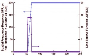
A particular column is selected (in this example column number 96), and all pixel values in this column are recorded to generate the SFR or Spatial Frequency Response.  The result of this operation is shown in Figure 2, with reference to the left vertical axis.

Figure 2 : Spatial Frequency Response, being the values of the pixels present in column 96 of the image shown in Figure 1, and Line Spread Function, being the first derivative of the SFR.

Next the LSF or Line Spread Function is generated, simply by numerically calculating the first derivative of the SFR.  The LSF is shown in Figure 2 as well, with reference to the right vertical axis.

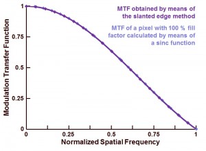
Once the LSF is known, the magnitude of the FFT of this LSF is calculated.  Plotting the FFT magnitude versus spatial frequency results in the MTF of the sensor, as shown in Figure 3.  Notice that the MTF is normalized with its value a zero input frequency (= DC), while the spatial frequency is normalized to the spatial sampling frequency of the sensor.  In this simulation example, the pixel pitch is equal to 6.5 µm.

Figure 3 : MTF of the simulated pixel (6.5 µm, 100 % FF), as well as the theoretical, geometric MTF of the same pixel.

In Figure 3 and next to the outcome of the MTF simulation, also the theoretical geometric MTF of the pixel is shown (6.5 µm, 100 % FF), for comparison reasons.  This geometrical MTF is calculated by means of the well-known sinc-function.  As can be seen, both curves coincide very nicely, indicating that the slanted edge method and the algorithms used in the calculation seem to do the job that they were developed for !

Before showing real measurements, in the next blog(s) a few additional improvements of the slanted edge method will be highlighted.

Albert, 18-06-2014.

How to Measure Modulation Transfer Function (3)

April 19th, 2014

A new measurement result in the MTF-series is shown in this blog : the MTF of a monochrome sensor, but no longer with white light input, but with red, green and blue light.  Some interesting observations can be reported.

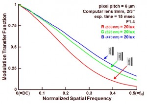
In Figure 1, the results of the MTF measurement are shown.

Figure 1 : Modulation Transfer Function of a monochrome device for various wavelengths of the incoming light.

It is quite nice to see the influence of the wavelength of the incoming light :

  • The absorption coefficient of silicon for “red” photons, or photons with a lower energy, is relatively low.  The absorption depth for light with a wavelength of 630 nm can reach a few microns.  So part of the electrons generated in the silicon will be generated below the depletion region of the photodiodes, and before these electrons can get collected by the photodiodes, they need to “travel” in the neutral bulk/epi-layer.  Because there is no electrical field present in these regions to guide the electrons to the right photodiodes, the chance that these electrons finally land in a neighbouring pixel is relatively large.  In this way the contrast in the image is reduced, so is the MTF,
  • The absorption coefficient of silicon for “blue” photons, or photons with a higher energy, is relatively large.  The absorption depth for light with a wavelength of 470 nm is just a few tens of a micron.  So most of the electrons generated in the silicon will be generated within the depletion region and the chance of diffusion of these electrons to neighbouring pixels is limited.  The contrast in the image is not reduced by the effect described above for the “red” photons, neither is the MTF,
  • The green light, with a wavelength of 525 nm, has an absorption coefficient situated between the red light and the blue light.  So not surprising that the MTF for the green light is lying between the blue and red results.

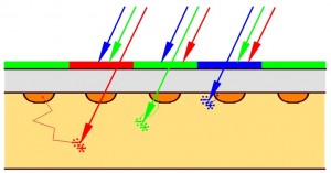
The effect explained here by means of the MTF measurements is also known as electrical cross-talk.  The loss in contrast or loss in MTF is due to the diffusion of electrons.  The effect is also illustrated in Figure 2.

 Figure 2 : Illustration of the electrical cross-talk.

Figure 2 shows a cross section of a hypothetical image sensor with an RGB filter.  Illustrated is the fact that the “red” photons can penetrated much deeper into the silicon than the “blue” ones.  This is the origin of the larger electrical cross-talk for the light having a longer wavelength.

To conclude a few numbers :

  • Absorption coefficient for a “red” photon (630 nm) = 4000/cm, resulting in an absorption depth of 2.5 um,
  • Absorption coefficient for a “green” photon (525 nm) = 10,000/cm, resulting in an absorption depth of 1 um,
  • Absorption coefficient for a “blue” photon (470 nm) = 20,000/cm, resulting in an absorption depth of 0.5 um.

Albert, 19-04-2014.

Announcement of the SECOND IMAGING FORUM, Dec. 11-12, 2014.

April 6th, 2014

Mark now already your agenda for the second solid-state imaging forum, scheduled for Dec. 11-12, 2014.

After the succesful first forum in 2013, I am happy to announce a second one.  Also this second solid-state imaging forum will be a high-level, technical, short course focusing on one particular hot topic in the field of solid-state imaging.  The audience will be strictly limited to 28 people, just to stimulate as much as possible the interaction between the participants and speaker(s).  The subject of the second forum will be : “Advanced Digital Image Processing”.

More information about the speaker and the agenda of the second forum will follow in the coming weeks, but I wanted to share this announcement with you as early as possible to make sure you can keep your agenda free on these days.

Albert,

April 6th, 2014.

How to Measure Modulation Transfer Function (2)

March 25th, 2014

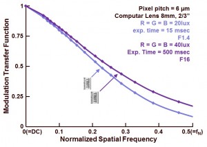
In the previous blog, the measurement of the Modulation Transfer Function by means of the Siemens star was explained.  In this blog, this method will be applied to check out the effect of the lens F-number on the MTF.

In Figure 1 the result of the MTF measurement is shown.


Figure 1 : Modulation Transfer Function for two settings of the lens F-number.

It is quite nice to see the influence of the F-number :

  • a low F-number is referring to a large lens opening (= a lot of light goes to the sensor, a short exposure time is needed), and in that case the incoming light is reaching the sensor with a large chief-ray angle (= deviation from the normal),
  • a large F-number is referring to a small lens opening (= much less light goes to the sensor, a long exposure time is needed), and in that case the incoming light is reaching the sensor with a small chief-ray angle (= almost perpendicular to the sensor).

Light that is perpendicularly reaching the sensor will suffer less from optical cross-talk in comparison to light that is reaching the sensor under a certain angle and is deviating more from the normal.  More (optical) cross-talk does result in less contrast between neighbouring pixels, thus lowering the MTF for larger spatial frequencies.  And this effect is observed in Figure 1 !

Next time something about colour and MTF.

Albert, 25-03-2014.

How to Measure Modulation Transfer Function (1)

February 20th, 2014

In a simple wording, the modulation transfer function or MTF is a measure of the spatial resolution of an imaging component.  The latter can be an image sensor, a lens, a mirror or the complete camera.  In technical terms, the MTF is the magnitude of the optical transfer function, being the Fourier transform of the response to a point illumination.

The MTF is not really the most easiest measurement that can be done on an imaging system.  Various methods can be used to characterize the MTF, such as the “slit image”, the “knife edge”, the “laser-speckle technique” and “imaging of sine-wave patterns”.  It should be noted that all method listed, except the “laser-speckle technique, measure the MTF of the complete imaging system : all parts of the imaging system are included, such as lens, filters (if any present), cover glass and image sensor.  Even the effect of the processing of the sensor’s signal can have an influence on the MTF, and will be include in the measurement.

In this first MTF-blog the measurement of the modulation transfer function based on imaging with a sine-wave pattern will be discussed.  It should be noted that in this case dedicated testcharts are used to measure the MTF, but the pattern on the chart should sinusoidally change between dark parts and light parts.  In the case a square-wave pattern is used, not the MTF but the CTF (= Contrast Transfer Function) will be measured.  And the values obtained  for the CTF will be larger than the ones obtained for the MTF.

The method described here is based on the work of Anke Neumann, written down in her MSc thesis “Verfahren zur Aufloesungsmessung digitaler Kameras”, June 2003.  The basic idea is to use a single testchart with a co-called Siemens-star.  An example of such a testchart is illustrated in Figure 1.
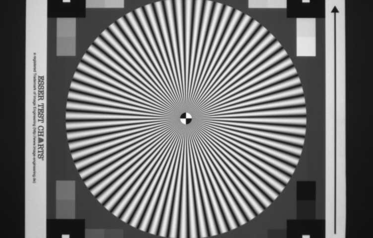
Figure 1 : Output image of the camera-under-test observing the Siemens star.

(Without going further into detail, the testchart contains more structures than used in the reported measurement performed for the MTF.)  The heart of the testchart is the Siemens star with 72 “spokes”.  As can be seen the distance between the black and white structures on the chart is becoming larger if one moves away from the center of the chart.  In other words, the spatial frequency of the sinusoidal pattern is becoming lower at the outside of the Siemens star, and is becoming higher closer to the center of the Siemens star.  Around the center of the Siemens star, the spatial frequency of the sinusoidal pattern is even too high to be resolved by the camera-under-test and aliasing shows up.  In the center of the Siemens star a small circle is included with 2 white and two black quarters.  These are going to play a very important role in the measurements.

The measurement procedure goes as follows :

  1. Focus the image of the Siemens star, placed in front of the camera, as good as possible on the imager.  Try to bring the Siemens star as close as possible to the edges (top and bottom) of the imager,
  2. Shoot an image of the testchart (in the example described here, 50 images were taken and averaged to limit the temporal noise).

In principle, these two steps is all one needs to be able to measure/calculate the MTF.  But to obtain a higher accuracy of the measurements, the following additional steps might be required :

  1. Cameras can operate with or without a particular offset corrected/added to the output signal.  For that reason it might be wise to take a dark reference frame to measure the offset and dark signal (including its non-uniformities) for later correction.  In the experiments discussed here, 50 dark frames were taken and averaged to minimize the temporal noise.
  2. The data used in the measurement is coming from a relatively large area of the sensor and is relying on an uniform illumination of the complete Siemens star.  Moreover, the camera is using a lens and one has to take into account the lens vignetting or intensity fall-off towards the corners of the sensor.  For that reason a flat-fielding operation might be needed : take an image of a uniform test target, and use the data obtained to create a pixel gain map.  In the experiments discussed her, 50 flat field images were taken and averaged to minimize the temporal noise.
  3. The camera under test in this discussion delivers RAW data, without any processing.  If that was not the case it would have been worthwhile to check the linearity of the camera (e.g. use of a gamma correction) by means of the grey squares present on the testchart as well.

Taken all together the total measurement sequence of the MTF characterization is then composed of :

  1. Shoot 50 images of the focused testchart, and calculate the average.  The result is called : Image_MTF,
  2. Shoot 50 flat field images with the same illumination as used to shoot the images of the focused testchart, and calculate the average image of all flat field images. The result is called : Image _light,
  3. Shoot 50 images in dark, and calculate the average image of all dark image.  The result is called Image_dark,
  4. Both Image­_MTF and Image_light are corrected for their offset and dark non-uniformities by subtracting Image_dark,
  5. The obtained correction (Image_lightImage_dark) will be used to create a gain map for each pixel, called Image_gain,
  6. The obtained correction (Image_MTF Image_dark) will be corrected again for any non-uniformities in pixel illumination, based on Image_gain.

If this sequence is followed, an image like the one shown in Figure 1 can be obtained.

  1. Next the pixel coordinates of the center of the testchart need to be found.  This can be done manually or automatically.  The latter is done in this work, based on the presence of the 4 quadrants in the center of the testchart.
  2. Once the centroid of the testchart is known, several concentric circles are drawn with the centroid of the testchart as their common center.  An example of these concentric circles on top of the testchart is shown in Figure 2.
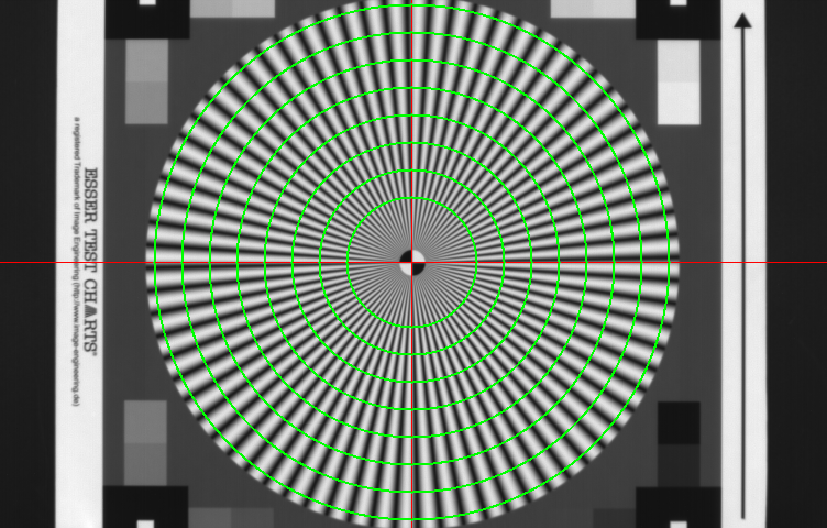
 

Figure 2 : Siemens star with concentric circles (shown in green), with their centers coincides with the centroid of the testchart (red cross).

  1. After creating the circles, the sensor output values of the various pixels lying on these circles are checked.  On every circle the pixel values change according to a sine wave, of which the frequency is known (72 complete cycles of the sine wave and it radius, in number of pixels, can be calculated).  For each of the circles, a theoretical sine wave can be fitted through the measured data.  Consequently for each circle a parameter can be found that corresponds to the amplitude of the fitted sine wave.
  2. In principle the MTF curve could be constructed, the only missing link is the value of the MTF for very low frequencies close to DC.  This value can be found as the difference between the white values and black values of the four quadrants right in the middle of the testchart.
  3. Normalizing the obtained data completes the MTF curve : the calculated amplitudes of the sine waves are normalized with the signals of the four quadrants in the middle of the chart, the frequencies of the sine waves are normalized to the sampling frequency of the imager (6 mm pixel pitch).

The outcome of the complete exercise is shown in Figure 3.
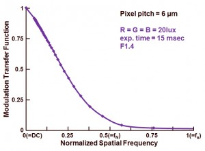
 Figure 3 : Modulation Transfer Function of the camera-under-test.

As indicated in Figure 3, the MTF measurement is done with white light created by 3 colour LED arrays (wavelengths 470 nm, 525 nm, 630 nm).  As can be seen from the curve, the camera has a relative low MTF, around 8 % at Nyquist frequency (fN).  In theory an imager with a large fill factor can have an MTF value of 60 % at fN.  But this camera is performing far away from this theoretical value.  But one should not forget, this MTF measurement does include ALL components in the imaging system, not just the sensor !

Now that the MTF measurement method is explained, in the next blogs more MTF results will be shown and compared.

Albert, 20-02-2014.
International Solid-State Circuits Conference 2014

February 12th, 2014


The image sensors’ harvest at the ISSCC 2014 was pretty weak this year.  Only half of a session was devoted to imagers.  In the past, 2 full sessions were filled with imager presentations …

Samsung presented their latest development in the field : a BSI-CMOS pixel with deep trench isolations/separations and with a so-called vertical transfer gate.

  1. The DTI is a very narrow, but very deep trench into the silicon.  These trenches completely surround the individual pixels.  Moreover they go through the complete sheet of silicon (after back-side thinned this is just a few microns).  The trenches seem to completely eliminate the optical and electrical cross-talk in the silicon.  CCM coefficients of devices without and devices with the DTI were shown, and the CCM of the DTI device comes much closer to the unity matrix.  This results in a much better SNR after colour processing.  The trenches seem to be filled with poly-silicon, which in its turn is isolated from the main silicon by an oxide.  Although not confirmed by the speaker, it is expected that the poly-silicon gates are used to bias the silicon of the pixel into accumulation to lower the dark current.  The dark current of the DTI pixel was equal to the dark current of the standard pixel without DTI.

    Because the pixels are 100 % isolated from each other, blooming is simply not possible.  This is an extra advantage of the DTI structure.

  2. The vertical transfer gate : the photodiode is not directly located at the silicon interface, but is buried into the silicon.  Above it, the transfer gate is located as well as the FD node.  So at the end of the exposure, the charges have to be transported upwards out of the diode into the FD node.  This buried diode results in a remarkably high full well of 6200 electrons for a 1.12 um pixel with DTI.

According to the speaker, Samsung is ready for the next generation of pixels below 1 um.  Two personal remarks :

  1. I would love to see this pixel in combination with the light guide between the colour filters, presented by Panasonic a few years ago at IEDM.  That should result in a device without spectral, optical and electrical cross-talk.
  2. These devices are great masterpieces of integration in the 3rd dimension, and not that much silicon is left anymore.

There was also a nice presentation by Microsoft of their ToF device.  They are using a non-conventional pixel : four toggling, small gates with wide open areas in between.  At the “head” of the gates, the FD nodes are located.  Pixels are being readout and processed in full differential mode and had the option to partly being reset during exposure.  This removes the background illumination.

The circuitry around the pixels allows the pixels to run at :

  • different shutter and different gain settings, resulting is an expanded dynamic range,
  • multiple modulation frequencies, solving the conflict of precision and depth range,
  • multi-phase operation, resulting in high accuracy and robustness.

The device realized has a depth accuracy of 0.5 % within a range of 0.8 m … 4.2 m.

Albert.

February 12th, 2014.

Electronic Imaging 2014 (2)

February 8th, 2014

Boukhayma (CEA-Leti) presented a very nice paper about the noise in PPD-based sensors.  He modelled the electronic pixel components for their noise performance, and based on this analysis he handed out some guidelines to limit the noise level in the pixels.  Although not all conclusions are/were new, it was nice to see them all listed in one presentation and supported by simulation results : lower the FD node capacitance, lower the width of the SF transistor, choose a p-MOS transistor as SF because an n-MOS transistor will give too much 1/f noise, optimize the length of the SF (depending on gate-drain capacitance, gate-source capacitance, FD capacitance and width of the transistor, the formula for the optimum gate length was shown).  If the thermal noise of the pixel is dominant, it does not matter whether to use a simple SF in the pixel or to use an in-pixel gain stage.  But if the 1/f noise is dominant, one should avoid a standard n-type MOS transistor.

Angel Rodriguez-Vazques (IMSE-CNM, Spain) gave a nice overview of ADC architectures when used for image sensors.  It is a pity that for such an overview paper only 20 minutes presentation time were provided.  These kind of overview papers deserve to get more time.

Seo (Shizuoka University, Japan) described a pixel without STI, but with isolation between the pixels based on p-wells and p+ channel stops.  The omission of the STI has to do with the dark current issues that come together with the STI.  The authors showed a very cute lay-out of a 2×2 shared pixel concept (1.75 T/cell).  All transistors and transfer gates were ring shaped, located in the center of the 2×2 pixel and with the 4 PPDs at the outside, looks a bit like a spider with only 4 legs.  The pixels were pretty large (7.5 x 7.5 um2), in combination with a relatively low fillfactor of 43 %, as well as a low conversion gain of 23 uV/electron.  Of course the ring structure of the output transistors consumes a large amount of silicon, and seems to result in a relative large floating diffusion capacitance.  The dark current is reduced by a factor of 20 (compared to the STI-based sensor), down to 30 pA/cm2, QE = 68% @ 600 nm.

It is hard to decide who will win the Award for the most artistic pixel lay-out : the hedgehog of Tohoku University or the spider of Shizuoka University ?  But it any case, the award goes to a Japanese university.  Great work !

Albert

February 7th, 2014.

Electronic Imaging 2014 (1)

February 7th, 2014

An interesting paper of Tohoku University was presented at the EI14.  They published their paper about a 20M frame/s sensor already a while ago at the ISSCC, but they never disclosed the pixel structure to empty the PPD within the extremely short frame times.  The EI14 paper was focusing on the pixel architecture and specifically on the PPD structure.  Miyauchi explained that two technological “tricks” are applied to create an electric field in the PPD to speed up the transfer of the photon-generated electrons from the PPD to the FD node.  Firstly a gradient in the n-doping is implemented by using three different n-dopings, secondly the n-regions are not simple rectangulars or a squares, but have the look of hedgehogs with all kind of sharp needles extending away from the FD node.  On one hand the lay-out of the triple n-implantation looks quite complicated, on the other hand it looks quite funny as well, but after all, it seems to be effective.

Simulations as well as measurement results were shown.  Simulated was a worst-case transfer time of 9ns, measured was a transfer time of about 5 ns.  These are very spectacular results taking into account that the pixel size is 32 x 32 um2.  As far as overall speed of the sensor is concerned : 10M frames/s are reported for a device with 100k pixels, 128 on-chip storage nodes for every pixel and a consumed power of 10W.  The device can also run in 50k pixels mode, with the same power consumption but then with a frame rate of 20M frames/s and with a storage capacity of 256 frames on-chip.


There were two papers that used the same image sensor concept : allow the pixels to integrate up to a particular saturation level, and record the time it takes to come to this point.  This idea is not really new (was it Orly who did this for the first time in her conditional reset idea ?), but the idea in which this concept is applied seems to be new.

El-Desouki (King Abdulaziz City for Science and Technology, Saudi Arabia) is using SPADs and is allowing the SPADs to count up its events to a certain defined number to convert an amount of light into a time slot, measures this time slot by converting it into the digital domain and is sending out this data.  A further sophistication of the idea is not to count in the digital domain (it needs too many transistors per pixel) but to do the counting in the analog domain.  Finally the author explained how one can make a TDI sensor based on this concept.

A bit more “out-of-the-box” was the concept introduced by Dietz (University of Kentucky).  Allow the pixels to integrate up to a certain level (e.g. saturation), record the time it takes to reach that point, and perform this action continuously in the time domain.  In this way one gets, for each pixel, a kind of analog signal describing the behavior of each pixel in the time domain.  This way of operating the pixel makes the sensor completely free of any frame rate.  If an image is needed, one can take whatever timeslot in the time domain that is recorded, take the analog signal out of the memory, and average the analog signal within this timeslot.  Of course every pixel needs a lot of processing as well as a huge storage space to record its behavior in the time domain.  But with the stacked concept of imager-processor-memory, the speaker was convinced that in the future this should be feasible.

Yonai (NHK, Japan) presented some new results obtained with the existing 33M UHDT sensor, already presented earlier in WKA winning paper.  But this time the authors changed the timing diagram such that the sensor was allowed to perform digital CDS off-chip.  Results : 50 times reduction in FPN (down to 1 electron) and 2 times reduction in thermal noise (down to 3 electrons @ 60 fr/s).

Kang (Samsung) presented some further sophistication of the RGB-Z sensor that was already presented by Kim at the ISSCC.  From one single imager, a normal RGB image can be generated, as well as a depth-map by using the imager in a ToF mode.  The author presented a simple, but intelligent technique to improve the performance of the device by removing any asymmetry in pixel design/lay-out/fabrication.  The technique applied is simply reversing the Q0 and Q180 from frame to frame.  Actually the technique looks very much the same as chopping in analog circuitry.


Albert

February 7th, 2014.