Archive for February, 2011

Imagers at ISSCC (5)

Monday, February 28th, 2011

Albert Wang (Cornell University) reported about “An Angle Sensitive CMOS imager for single-sensor 3D photography”.  Very interesting new technology in the 3D world.  An image sensor is described that is capable of detecting the direction of the incoming rays, and based on that, the object distance can be calculated.  In other words, a depth map can be created.  The main application for this sensor are ranging and computational refocus. 

The sensor itself is based on a regular CMOS device overlaid with two grids (made in M3 and M5).  A kind of interference effect is generated by means of these two grids depending on the angle of the incoming rays.  The overall working principle is based on the so-called Talbot effect, published (and referenced !!) in 1836.  [Talbot is also the bass player of Crazy Horse, the band of Neil Young. It remains a small world]

To become a commercial product, still a long way needs to be travelled I guess, but it is a very appealing concept because it does not need any extra laser pulse, and makes use of the direct incoming information through standard lenses.  Something to watch.

Also a nice concept is the next paper by Robert Johansson (Aptina) : “A 1/13-inch 30fps VGA SoC CMOS image sensor with shared reset and transfer gate pixel control”.  The basic question is : how to further optimize the fillfactor of a front-side illumination 4T pixel ?  After putting them into a 2 x 1 shared concept, the number of metal lines going into the pixel is further reduced to 1 vertical line (column bus sharing the supply line) and 1 horizontal line (reset of line n+1 is shared with the transfer gate of line n).  The sharing makes the timing a bit more complex, but that is just a matter of developing once and you’re done. 

To further reduce the overall chip size, the black reference columns and lines are replaced by a small 2D area (48 x 17 pixels) to generate a black reference.  Some of these pixels have the transfer gate active, others do not.  This allows to get a fairly good idea about the dark current generation.  Some performance numbers : CF = 272 uV/electron, read noise at maximum gain = 1.68 electron, pixel capacity at max linear range = 3400 electrons.  These numbers hold for a pixel of 1.75 um pitch and a fabrication technology of 0.11 um.  Total power consumption is 55 mW (but frame rate is not mentioned).

“A 1/2.33-inch 14.6M 1.4 um pixel backside illuminated CMOS imager sensor with floating diffusion boosting ” by Sangjoo Lee (Samsung) support the continuous effort in back-side illuminated devices.   Thanks to the BSI, more circuitry can be afforded on the front-side, and for that reason extra FD boosting circuitry was included.  This gave an extra boost of 0.67 V on the FD at a boosting pulse of 4 V (? not sure if this is correct).  It was mentioned during the talk that the crosstalk of the BSI was equal to the FSI situation, but no numbers were mentioned.  A nice cross section of the silicon was shown, clearly indicated a very low optical stack at the backside, and no metal grid at the backside.   The noise level was down to 1.4 electron (speed ?), a full well of 5700 electrons and the SNR10 improved from 135 lux for the FSI to 87 lux for the BSI. 

Very nice work and another one who is ready to join the BSI club.

“An APS-C format 14b digital CMOS image sensor with a dynamic response pixel” by Dan Pates (Aptina).  To start with, the dynamic response pixel refers to a dual conversion gain in the pixel by the possibility to add an extra capacitor to the floating diffusion or not.  The pixels of this sensor are pretty large (4.78 um) and thus more freedom and space is available to play around with the design.  The presenter showed three different ring gate structures that avoided STI in the pixel area for isolation.  These ring structures look very similar to radiation tolerant pixel designs, and also in this case the main reason to avoid STI is to reduce the dark or leakage current.  In the reported numbers this low dark current (17 electrons at 60 deg.C) was shown, as well as a lower noise level (16 electrons at low gain 1x, 2.2 electrons at high gain 8x), a large fill factor, high sensitivity (49.5 kelectrons/lux.s)  and large full well (50 kelectrons at low gain and 16 kelectrons at high gain). 

The ADC implemented is based on SA, and contains 14 bits.  Overall frame rate is 10.48 fps. 

The last paper in the imaging session of ISSCC2011 was “A 17.7 Mpixel 120 fps CMOS image sensor with 34.8 Gb/s readout” by Takayuki Toyama (Sony).  The sensor reported was on based on the “classical” Sony concept of column parallel ADCs based on up-down counters.  But because of the extremely high bitrate of the overall chip, the 14 counters in the column are split into two parts :

       The lower 5 bit counters, which are driven with 248 columns in parallel, in such a way that the columns do not contain the real counters, but contain memory cells,

       The upper 9 bit counters, which are based on real counters as before.

This hybrid construction allows to maintain the high accuracy of 14 bits with the extremely high speed of 34.8 Gb/s overall.  The device runs at 120 fps at 12 bits and 60 fps at 14 bits.  The chip is realized in 90 nm technology, 1P4M and consumes a total power of 3W at 120 fps.

Overall conclusion of this imaging session : the technical committee put a great set of papers together.  Not just the content of the papers were high level, so was the presentation of the papers.  Congratulations to all authors, I really enjoyed a great Wednesday morning !

Albert, 28-02-2011.
Imagers at ISSCC (4)

Friday, February 25th, 2011


Prof. Etoh of Kinki University presented a new member of its high-speed camera family : “A 16Mfps 165 kpixel Backside-Illuminated CCD”.  This device captures the information at 16 Mfps and stores them on-chip.  The on-chip analog memory can hold 100+ images.  During the presentation very nice demo videos were shown.

This new device is a back-side illuminated one, because with 16 Mfps the sensitivity is becoming an issue.  To actually shield the on-chip analog memories from incoming back-side light, a new architecture of multiple n- and p-wells is developed on more or less thick epi-layers (top n-epi of 9 mm, bottom p-epi of 23 mm).

Personally I know prof. Etoh very well because in my Philips career I worked together with him.  What I admire so much about this person is the fact that he is a civil engineer specialized in water engineering !  He has no electrical engineering background, but he designs very advanced image sensors.  This is a great example of “thinking out of the box”.  On the other hand he shows that our analogy of potential wells with buckets on one hand, and the electrons in the wells with water in the buckets on the other hand helped him to develop very advanced imaging structures.

Next in line was Y. Yamashita (Canon) with “A 300mm Wafer Size CMOS Image Sensor with In-Pixel Voltage Gain Amplifier and Column-Level Differential Read-out Circuitry”.  Apparently this was the ISSCC of the world records : after a world record in speed, this must be a world record in size !  The imager has a size of over 20 cm by 20 cm !  Number of pixels is relatively low (1280 x 1248), so the pixels are very large, 160 mm x 160 mm, as a consequence, they can easily contain some extra electronics.  On the other hand, the bus capacitances of such a large imager are huge, so extra buffer electronics are a must in every pixel.  The application for this huge imager are night vision and astronomy.  Of both, examples and videos were shown.  Very impressive of course.

Because of the large pixel and the extra amplification in every pixel, the sensitivity is huge, namely 25 Melectrons/lux.s, as well as the conversion gain, being 318 mV/electron.  Noise level is reported to be 13 electrons rms with a maximum power consumption of 3.2 W.  The spec indicates that the maximum frame rate is 100 fr/s, but it is not mentioned whether the noise and power figure were measured at this maximum frame rate.

R. Walker (University of Edinburgh) reported about his PhD project : “A 128 x 96 Pixel Event-Driven Phase-Domain D?-Based Fully Digital 3D Camera in 0.13 mm CMOS Imaging Technology”.  This work was done in collaboration with ST, and is the very first fully integrated 3D camera on a single chip.  The generation of the depth map is fully integrated on the chip itself !

The pixels of this chip are based on SPADs.  But to avoid the enormous amount of data that can be generated by a SPAD, every pixel includes next to the SPAD an all-digital phase-domain delta-sigma implementation with 6 bit counters for partial in-pixel decimation.  The pixels are pretty large, 44.65 mm pixel pitch, and in combination with the 0.13 mm technology, some extra electronics can be afforded in every pixel.  A remarkable low power consumption was reported, only 40 mW.  Unfortunately I cannot post the presentation slides (because I do not have them) and I am not allowed to post them (because of the copyrights), but the presenter did a great job in explaining the working principle of the chip by means of a great set of slides.

MORE TO COME !

Albert, 25-02-2011.

Imagers at ISSCC (3)

Thursday, February 24th, 2011


Wednesday morning, Feb. 23rd, the imaging session was schedule.  Find here the first reviews.

M.W. Seo ( Shizuoka University) presented : “An 80mVrms Temporal Noise 82 dB Dynamic Range CMOS Image Sensor with a 13-to-19b Variable Resolution Column-Parallel Folding-Integration/Cyclic ADC”.  This is not the first time that this group is presenting a column-level ADC for CMOS image sensors, but they keep improving the noise performance.  During the presentation the author showed a nice overview of the work done by this group and how the performance was constantly improved.  The target spec for this device was : < 1 electron noise, 80 dB dynamic range and 18 bits ADC.  What was realized : 0.95 electron noise (at 128 times sampling), 82 dB (with 64 times sampling and up to 19 bits ADC.  The ADCs do have the option for multiple sampling and that results in an improved noise performance.  Unfortunately that goes together with a reduction of the frame rate.  The author explained the circuitry and working principle of the ADC, but that is too complex (for me) to explain in this short review.  During the Q&A the author mentioned that the limitation of the noise floor is now the 1/f noise, as well as the power dissipation being 415 mW at 19 bits.  The device is a 1Mpixel test imager with a pixel pitch of 7.5 mm.

Next in line was C. Lotto (Heliotis) to present a nice pixel based on 4T (1 nMOS and 3 pMOS).  The pixel can switch between two modes by clever re-coupling of the circuitry : closed loop reset mode (to keep the effect of FPN and spread on threshold low) and open loop amplifier mode (to add amplication in the pixel).  Also this pixel realizes a noise floor lower than 1 electron, namely 0.86 electron (at RT and at 60 fr/s of 256 x 256 pixels), with a conversion gain of 300 mV/electron.  Despite the extra gain in the pixel, the PRNU could be kept down to 2.5 % and the linearity error could be kept below 1.7 %.  Also in this presentation is was stated that the limiting noise floor for the pixel is the flicker noise.

The two devices presented so far, both with a noise level below 1 electron, were both fabricated in 0.18 mm technology.  The imager session started with two papers indicating the psychological barrier of 1 electron noise is not that far away anymore. 

Albert, 24-02-2011.

Imagers at ISSCC (2)

Wednesday, February 23rd, 2011


Due to business reasons I had to skip the ISSCC on Tuesday.  But I am very delighted that Dan McGrath wrote a short note about the imaging papers presented during my absence.  A big “thank you Dan !”.

So, here is the report written by Dan :

Three comments related to imaging for Tuesday ISSCC.


(1) Paper from C. Veerappan (cooperation between Delft University of Technology, STMicroelectronics, University of Edinburgh, Fandatione Bruno Kessler and EPFL) an described a 160×128 image sensor based on a SPAD pixel with in pixel circuitry to allow time-to-digital conversion. Fluorescent tags were differentiated by characterizing their time dependent decay through imaging multiple frames, in the process removing factors that limited the precision. The target application is fluorescent imaging (FLIM) to facilitate looking not just at the surface, but also into processes happening below the surface of biological samples (e.g., pollen grain). 10-bits were achieved by a combination of a ring oscillator and a thermometer code converter and alternative readout and evaluation modes were enabled by the circuitry. The price paid for this circuitry was a 2% fill factor and the need  to work to compensate for this thru the design of microlenses. The time jitter limitations were stated to result from the characteristics of the photodiode, not the circuitry.


(2) Paper by B. Richter (Fraunhofer Institute for Photonic Microsystems) described a VGA OLED display built on a transparent substrate with each pixel consisting of a small photodiode surrounded by an display element. The target application is a heads-up display where the user interface is managed by having the integrated image array track eye motion. The value of such a system is that it can be used when hand motion is not available, such in driving a car in hazardous conditions or in surgery. The application requires sophisticated optics based on the use of visible light for the display function and infrared light for the eye tracking, with beam splitting to allow the heads up function and with optics that differentiates between the wavelengths to provide the proper focal length for each function. This is similar to a Samsung paper presented several years ago at ISSCC, but where the imaging was used for a touch screen so that there was not the problem of the optical design.


(3) The evening session discussing the promise of the smart grid providing an information and control portal into the home for the homeowner and the utility appeared only to mention imaging once and then as aside in the form of a mention of security cameras. The bulk of the sensing and information gathering was non-imaging sensing of electrical loads and voltages and of motion sensors. Imaging appears to be something you carry with you, but not something that works humbly in the home.


Albert (& Dan), 23-02-2011 


Imagers at ISSCC (1)

Tuesday, February 22nd, 2011

Today, Feb. 21st, 2011, the International Solid-State Circuit Conference started.  On this first day, there were two interesting presentations about image sensors :

Bart Dierickx (Caeleste) presented a paper : “Indirect X-ray Photon-Counting Image Sensor with 27 T Pixel and 15 electrons Accurate Threshold”.  The paper started with the explanation of direct and indirect detection.  In the case of indirect detection the X-ray is absorbed in a scintillator, and is generating a cloud of visible photons which are detected by the underlying imager.  In the (test-)chip presented, the pixels are based on a photodiode that is detecting the incoming cloud of scintillator-generated photons.  After absorbing the latter, the photodiode generates a pulse corresponding to 100 up to 500 electrons.  The in-pixel circuitry creates out of the burst signals of the photodiode a digital pulse train which are counted in the pixel itself.  The nice thing about this counter it its implementation as an analog part.  This consumes only a very small part of the pixel real estate.  Unfortunately this was only a short paper and the presenter could not go into detail about the performance of the analog counter.  Would have been interesting to hear something about linearity and other performance parameters. 

The paper concluded with measurement results and a look into the future.  It clearly showed the ability of detecting single X-ray photons.  Apparently the next focus will be on the shrinkage of the pixels, increase performance, as well as increasing functionality.  (Where did I heard this before ?)

The second imager paper was delivered by Suat Ay (University of Idaho, ID) : “A 1.32 pW/frame.pixel 1.2 V CMOS Energy-Harvesting and Imaging (EHI) APS Imager”.  Quite funny idea in which the imager itself tries to collect the energy that it needs to support its own operation.  That captured energy is the incoming light itself.  Primary application is an artificial retina.

The pixel used is based on a 3T architecture, with a double photodiode : the first (classical) one is used for the integration of the incoming light information, and the second one is operating in the solar cell mode.  In the imaging mode, the solar cell diode is connected in parallel to the first diode to increase the sensitivity.  In the design/lay-out, the imager photodiode is a p+/n-well diode, while the energy harvesting diode is an n-well/p-sub diode.  So they are optimally stacked in the pixel to allow a maximum fill-factor for both.  During the presentation the author showed very nice sheets to illustrate the switching between the two modes of operation : imaging and energy harvesting.  Unfortunately these sheets are not published in the conference proceedings. 

As can be understood, the amount of generated power will be small, so has to be the amount of power consumption by the imager itself.  In imaging mode, the device consumes 14 mW at full speed (7.5 fr/sec, 54 x 50 pixels, 10 bit SAR ADC, digital timing off-chip), in energy harvesting mode the device consumes 6.7 mW and is able to harvest 2 mW of energy and to store this on an external capacitor.  These numbers are valid under normal daylight.  This means that the device is able to harvest the energy with an efficiency of 9 %.  The imager is made in 0.5 mW technology and the pixels are 21 mm x 21 mm.  Some other data not shown in the proceedings : saturation level of 0.7 V, full well of about 400,000 electrons, floating diffusion capacitance of 91 fF, noise level of 460 electrons (mainly kTC noise of the 3T pixel with a large capacitance and operated in non-correlated double sampling) and a responsivity to light of 0.4 V/lux.s.  Despite the large noise floor and the very low supply voltage of 1.2 V the sensor is able to deliver a dynamic range of 58 dB. 

Albert, 21-02-2011.


Number of Photons and PTC

Tuesday, February 8th, 2011


Another interesting parameter to investigate is the amount of photons that are falling on a pixel ?  So in this blog we will vary the amount of light, expressed in the number of photons, coming to the sensor.  In a practical situation this simply means that the incoming light power needs to be measured and next, the amount of photons needs to be calculated (knowing the wavelength of the incoming light).   Based on the synthetically generated images, the FPN and the temporal analysis is performed, in the same way as also done earlier in previous blogs.

For this experiment, the amount of photons was changed in multiple steps from 0 to 6.5 Mphotons.  In this way a varying light input can be generated.  Actually this is already being done in an earlier blog by changing the exposure time of the sensor.  It can be expected that the results are very similar to the ones obtained when working with different light inputs through changing the exposure time, but here we can get something extra.  The results are shown in 4 figures :

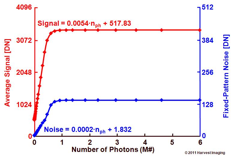
Figure 1 showing the average signal and the light fixed-pattern noise as a function of the amount of incoming photons.  As can be expected the average signal as well as its FPN component increase as a function of the number of photons.  In this particular example, the exposure time is fixed to 100 ms, making sure that the pixels easily saturate at the higher photon flux values. 

110207_blog_1


Figure 1 : average signal and light fixed-pattern noise as a function of the amount of incoming photons.

As can be expected, in the non-saturated situation, the output signal is proportional to the amount of incoming light.  Shown in Figure 1 is the relation between the output signal and the number of photons, as well as the FPN as a function of the number of photons.  The ratio between the two formulas reveals the FPN in light, or the PRNU, being equal to : 0.0002/0.054 = 0.037 or 3.7 %.

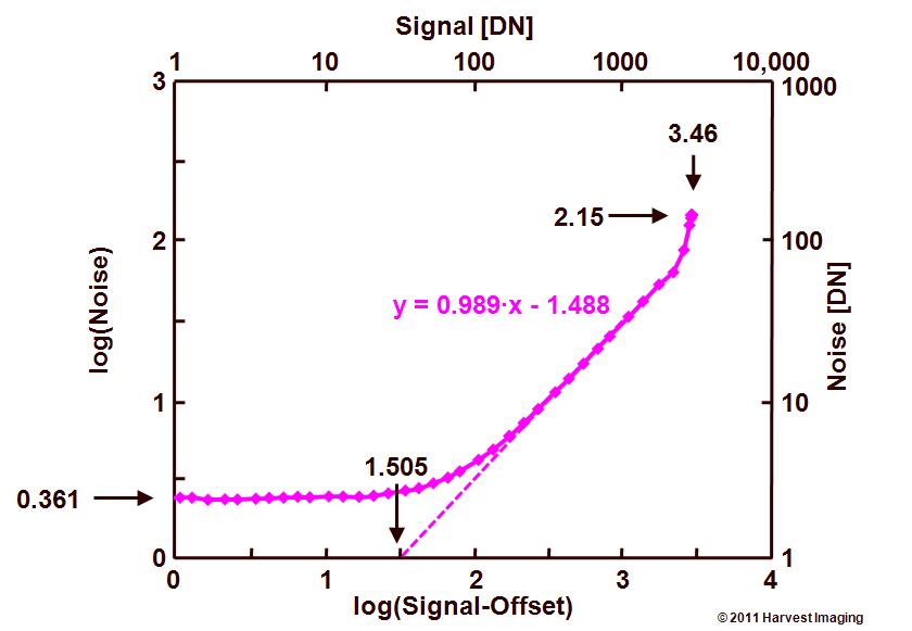
Figure 2 showing the light fixed-pattern noise as a function of the average effective output signal.

110207_blog_2


Figure 2 : light fixed-pattern noise or PRNU as a function of the average effective output signal.

From this figure the following parameters can be extracted :

       FPN on pixel level being equal to 100.361 DN = 2.30 DN,

       The saturation level being equal to 103.46 DN = 2884 DN,

       The PRNU level being equal to 10-1.505 = 0.031 or 3.1 %.

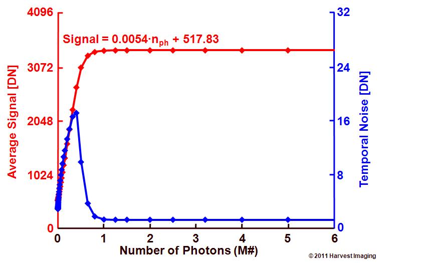
Figure 3 showing the average signal and its temporal noise component as a function of the light input.

110207_blog_3


Figure 3 : average signal and temporal noise as a function of the light input.


The average output signal curve is the same as the one in Figure 1, but the noise shown is now the temporal noise, basically composed out of photon shot noise as long as the pixel is not saturated. 

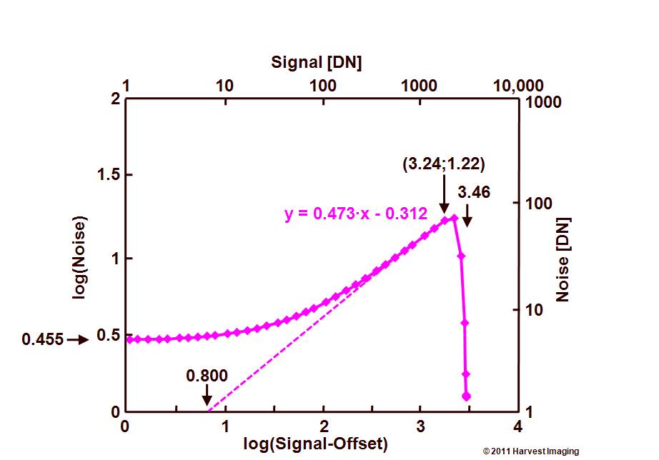
Figure 4 showing the temporal noise as a function of the average signal.

110207_blog_4


Figure 4 : temporal noise as a function of the average effective output signal, or the Photon-Transfer Curve.

This last figure is showing the real and original photon-transfer curve.  From the graph the following details can be deduced :

       Noise floor in dark being equal to 100.455 DN = 2.85 DN,

       Onset of anti-blooming at 103.24 DN = 1738 DN,

       Saturation level being equal to 103.46 DN = 2884 DN,

       Conversion gain, being equal to 10-0.800 = 0.158 DN/e.

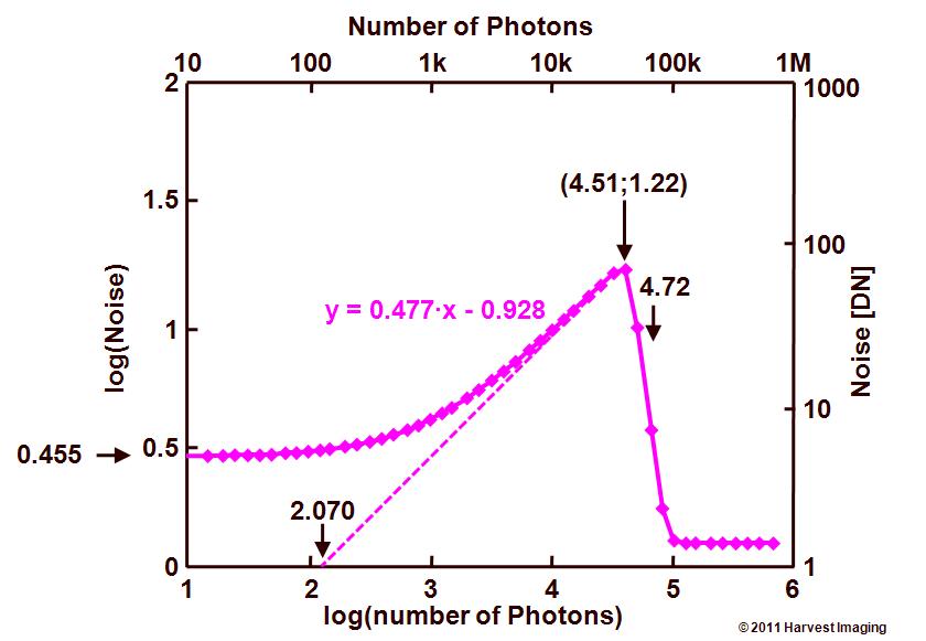
As can be learned from this short exercise, the amount of incoming photons can be a parameter of interest to change the input signal to the sensor and to generate the data needed to reconstruct the PTC curve.  It should be noted that there is no need to know the exact amount of photons to construct figures 2 and 4.  So the variation in photons can be realized by whatever means you have available.  But in the case that the exact amount of photons can be measured, it is worthwhile to create the PTC with the number of incoming photons on the horizontal axis instead of the effective output signal.  This curve is shown in Figure 5.

110207_blog_5


Figure 5 : temporal noise as a function of the amount of incoming photons.

Going back to the formulas derived to generate the PTC, the effective output signal can be written as :

                                   Stot = k·No = k·h·Nph

with :

       Stot : the effective output signal (corrected for the offset),

       k : conversion gain,

       No : number of electrons generated in the pixel,

       h : quantum efficiency of the pixel,

       Nph : number of photons impinging the pixel.

The noise can be written as :

                                   stot = k·stemp = k·(sr2 + so2)0.5 = k·(sr2 + h·Nph)0.5

with :

       stot : total noise measured at the output of the sensor,

       stemp : temporal noise on pixel level,

       sr : noise floor of the electronic circuitry,

       so : photon shot noise.

In the case the noise floor of the electronic circuitry is the dominant noise source, the total measured noise simply equals to :

                                   stot = k·stemp = k·sr

but when the system is shot-noise limited, the noise equals to :

                                   stot = k·(h·Nph)0.5

or for stot = 1, one finds :

                                   h = 1/(k2·Nph)

which adds to the PTC the option to calculate and measure the quantum efficiency.  Unfortunately in this situation the PTC looses one of its most attractive features : it is no longer a relative measurement, absolute measurements of the light input is mandatory.

In the case of Figure 5, the quantum efficiency can be found as :

h = 1/(0.16·0.16·102.07) = 0.332 = 33.2 %.

Good luck with your own experiments.

Albert, 07-02-2011.