Archive for February, 2020

ISSCC2020 (3)

Sunday, February 23rd, 2020

“A 0.8V multimode vision sensor for motion and saliency detection with ping-pong PWM pixel” by the National Tsing Hua Univ., Taiwan.

Energy-efficient always-on motion detection (MD) sensors are in high demand and are widely used in machine vision applications.  To achieve real-time and continuous motion monitoring, high speed low-power temporal difference imagers with corresponding processing architectures are widely investigated.  Event-based dynamic vision sensors (DVS) have been reported to reduce the redundant data an power through the asynchronous timestamped event-address readout.  But these sensors need special data processing to collect enough events for information extraction.  Noise and dynamic effects can be issues as well.  Frame-based MD rolling shutter sensors were reported to reduce the data bandwidth and power by sub-sampling operation, global shutter MD sensors were reported using in-pixel analog memory for reference image storage.  In a frame-based MD sensor, the required analog processing circuit and two successive frames for temporal difference operation comes at a cost in power, area and speed.  In this paper a frame-based MD vision sensor is presented, featuring three operation modes :

  • Image capture,
  • Frame-difference with on/off event detection,
  • Saliency detection.

Using a low-voltage ping-pong PWM pixel and multi-mode operation, it achieves high-speed low-power full resolution motion detection, consecutive event frame reporting, and image capture features.  Moreover, saliency detection by counting the block-level event number is also implemented for efficient optic flow extraction of the companion processing chip using simple neuromorphic circuits.


“A 1280×720 back-illuminated stacked temporal contrast event-based bision sensor with 4.86 um pixels, 1.066 GEPS readout, programmable event-rate controller and compressive data-formatting pipeline” by Prophesee and Sony.

Event-based (EB) vision sensors pixel-individually detect temporal contrast exceeding a preset relative threshold to follow the temporal evolution of relative light changes and to define sampling points for frame-free pixel-level measurement of absolute intensity.  EB sensors gain popularity in high-speed low-power machine vision applications thanks to temporal precision of recorded data, inherent suppression of temporal redundancy resulting in reduced post-processing cost, and wide intra-scene dynamic range operation.

The heart of the pixel is a logarithmic responding photodiode, and every time the pixel exceeded a certain threshold in amplitude, the pixel detects “an event”.  Events can be positive and negative.  This concept is illustrated below.

ISSCC_5

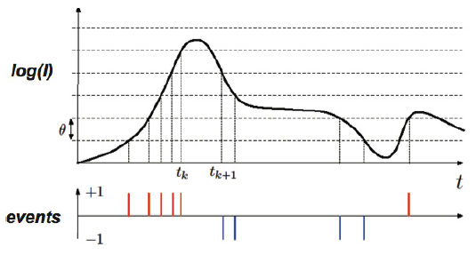
The photodiode is partially pinned and the logarithmic response is realized by means of a subthreshold MOS based logarithmic photocurrent-to-voltage converter.  The chip is making use of stacking technology with a per-pixel interconnect.  The toplayer (90 nm BI CIS) consists of the photodiode plus 2 nMOS transistors, all other pixel circuitry (50 transistors) are located on the bottom layer (40 nm CMOS).  Pixel pitch is 4.86 um with a fill factor of over 77 %.  The overall power consumption of the chip depends on the number of events that are detected, e.g. at 100 kEPS the chip consumes 32 mW, at 300 MEPS, power consumption is equal to 73 mW.

The latter paper got a lot of attention, not just because of the device performance, but also because of the remarkable cooperation between the two companies.

Albert, 23 February 2020.

ISSCC2020 (2)

Thursday, February 20th, 2020

“A 1/2.65inch 44Mpixel CMOS image sensor with 0.7 um pixels fabricated in advanced full-depth deep-trench isolation technology” by Samsung.  Basically the title says it all.

Remarkable technology that is used to create the deep-trenches in a pixel of 0.7 um.  On the backside of envelope I calculated the trench should be around 85 nm in width, with an aspect ratio of 69.  Next an isolation is provided on the sides of the trenches and the poly-Si filling takes place.  For the latter it is even more challenging : the aspect ratio is increased to 110.  It is really incredible that these things are possible in CMOS technology.

Some numbers :

  • Pixel size : 0.7 um,
  • Full well : 6000 electrons,
  • Temporal noise : 1.4 electron,
  • Dark current at 60 deg.C : 1.3 electron.

It is not just the trenches that are further optimized in the technology (compared to the 0.8 um pixel pitch that is most probably used in the 108 Mpixel device), also the boxing of the CFA is changed : a low refractive index grid is used instead of tungsten.  This results in an increase of about 15 % In QE(green).

The sensor presented is making use of the quad Bayer structure.  This is a very attractive architecture for binning options.  With binning the SNR can be increase considerably for applications in harsh light conditions (at the expense of resolution of course).  The results are shown in the figure below.

ISSCC_4


Artilux presented “An up-to-1400 nm 500MHz Demodulated time-of-flight image sensor on a Ge-on-Si platform”.  It is of course well known that the silicon response is limited up to a wavelength of 1100 nm.  If one is interested in detection of longer wavelengths, another material than silicon is needed, for instance germanium (Ge).

The reason to go for longer wavelengths, such as in time-of-flight applications, can be found in :

  • issues with eye-safety between 800 nm and 1100 nm,
  • background sunlight : the sun does not emit at 1300 nm.

If one compares the absorption spectrum of germanium with the one of silicon, indeed germanium seems to be a viable candidate to replace silicon for longer wavelengths.  The paper presented puts a very thin Ge toplayer on a silicon readout circuit.  The idea is not really new, this was already done earlier by Noble Peak (USA).  A cross section of the Si readout structure provided with a thin Ge layer (using a Si carrier ?) is shown below.

ISSCC_3

The authors claim to reach a QE equal to 50 % at 1500 nm and further optimization is still possible in optimizing the microlenses for this wavelength.  Nevertheless, there still some work needed to lower the dark current.   In the ToF application a modulation depth of 90 % can be obtained at 500 MHz modulation frequency, resulting in a measurement error less than 0.5 % for a distance of 1 m.

Albert, 20 February 2020.


ISSCC2020 (1)

Wednesday, February 19th, 2020

ISSCC 2020 (1)

A few words about the imaging papers at the International Solid-State Circuits Conference 2020.  Let’s get started with an easy one.

Sony presented a paper “A 132 dB single exposure dynamic range CMOS image sensor with high temperature tolerance”.  This paper is an extension of the one presented at IEDM 2018.  This pixel of IEDM 2018 is composed out of two photodiodes (small one for highlights, big one for lowlights).  At the IEDM 2018 version, they were making use of three different sensitivity levels to create the high dynamic range.  In the ISSCC2020 version, an extra sensitivity level is added to create a high dynamic range by means of four different sensitivity levels.  So in total two photodiodes, the large one has two conversion gains, the small one has a single conversion gain, with the capability of overflow to an in-pixel capacitor.  To operate the device in low noise, 8 readout cycles per pixel are needed, because for every signal (low/high conversion gain, small/large photodiode) also a reference signal readout is needed.  The area ratio between the two photodiodes is reported to be 14.5, in the 2018 version, this ratio was 10.

The pixel structure is shown in the following figure (FC is the newly added capacitor) :

ISSCC_1

Some numbers :

  • Pixel pitch : 3.0 um,
  • FE 90 nm, BE 65 nm (1P4Cu), logic part :40 nm (1P6CU,1AL),
  • Highest full well : 165,800 electrons, (this high full well is reached thanks to a vertical transfer gate instead of the classical planar one).
  • Random noise 0.6 electrons,
  • Single exposure (multiple reads) dynamic range : 132 dB.

The device is fabricated in a stacked technology, connection between the top and bottom layer is done on column level (TSV ?)

The title also refers to a high temperature tolerance, but in the presentation nothing was mentioned what has being done to obtain this high temperature tolerance, neither what was the gain in temperature tolerance w.r.t. other devices.

A global shutter paper was presented by Samsung : “A 2.1 e temporal noise and -105 dB parasitic light sensitivity backside-illuminated 2.3 um pixel voltage domain global shutter CMOS image sensor using high-capacity DRAM capacitor technology”.  These days the titles of these talks are so long that actually all ingredients of the talk are already included in the title.

The paper is concentrating on the voltage domain global shutter option with correlated double sampling in the pixel.  The authors referred to the issues with parasitic light sensitivity of the storage node in a charge domain global shutter and to the issues with kTC noise in the voltage domain global shutters if the storage capacitors are too small.  The latter is solved in this paper by incorporating a high-capacity DRAM storage capacitor on top of the pixel.  Because the technology is BSI, “plenty” of room is available to build an extra capacitor at the front-side of the pixel.  This capacitor is not a stacked one, it is realized during the CMOS fabrication on top of pixel, in the third dimension.

The pixel itself has a classical structure that is known for voltage domain global shutter pixels, but a few extras are added : an extra transistor between the floating diffusion and the reset transistor to create a dual conversion gain, a clamping transistor to perform in-pixel CDS (based on clamping) and an extra capacitor that allows to short-circuit the in-pixel CDS and storage node, and actually allows the pixel to operate in the rolling shutter mode.

The device realizes the following performance :

  • Pixel size 2.3 um,
  • Stacked BSI (but the DRAM capacitor is not stacked !)
  • Saturation level 12000 e at low gain
  • PLS : -115 dB (green)
  • Performance at 940 nm : PLS = -95 dB, QE = 42 %,
  • Read noise : 2.1 e for 18 dB of gain,
  • Frame rate : 120 fps.

The heart of this pixel is of course the DRAM capacitor on top of the front side of the pixel, a cross section is shown below :

ISSCC_2

(more to follow)

Albert, 19 February 2020.