“A 1/2.65inch 44Mpixel CMOS image sensor with 0.7 um pixels fabricated in advanced full-depth deep-trench isolation technology” by Samsung. Basically the title says it all.
Remarkable technology that is used to create the deep-trenches in a pixel of 0.7 um. On the backside of envelope I calculated the trench should be around 85 nm in width, with an aspect ratio of 69. Next an isolation is provided on the sides of the trenches and the poly-Si filling takes place. For the latter it is even more challenging : the aspect ratio is increased to 110. It is really incredible that these things are possible in CMOS technology.
Some numbers :
- Pixel size : 0.7 um,
- Full well : 6000 electrons,
- Temporal noise : 1.4 electron,
- Dark current at 60 deg.C : 1.3 electron.
It is not just the trenches that are further optimized in the technology (compared to the 0.8 um pixel pitch that is most probably used in the 108 Mpixel device), also the boxing of the CFA is changed : a low refractive index grid is used instead of tungsten. This results in an increase of about 15 % In QE(green).
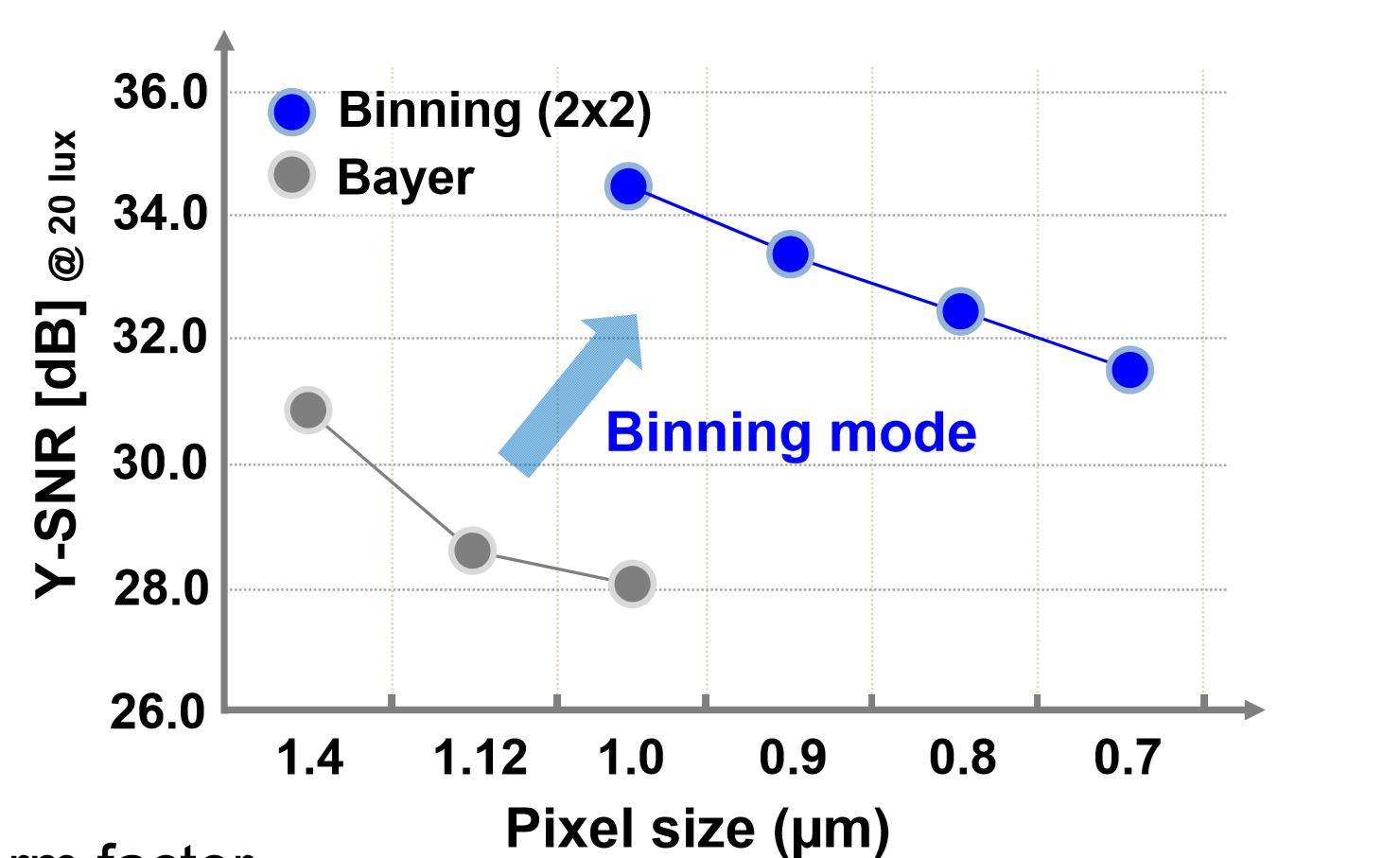
The sensor presented is making use of the quad Bayer structure. This is a very attractive architecture for binning options. With binning the SNR can be increase considerably for applications in harsh light conditions (at the expense of resolution of course). The results are shown in the figure below.
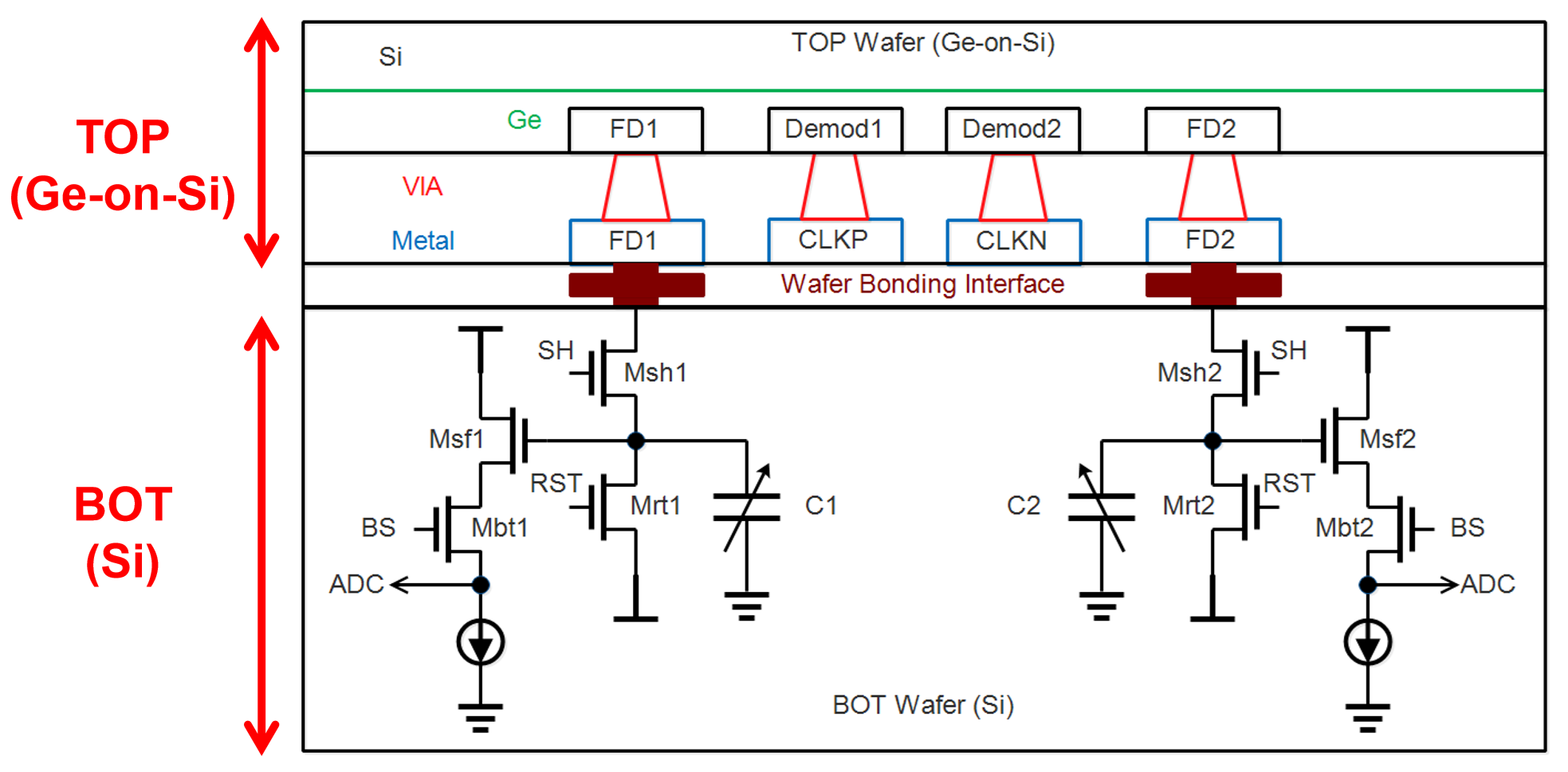
Artilux presented “An up-to-1400 nm 500MHz Demodulated time-of-flight image sensor on a Ge-on-Si platform”. It is of course well known that the silicon response is limited up to a wavelength of 1100 nm. If one is interested in detection of longer wavelengths, another material than silicon is needed, for instance germanium (Ge).
The reason to go for longer wavelengths, such as in time-of-flight applications, can be found in :
- issues with eye-safety between 800 nm and 1100 nm,
- background sunlight : the sun does not emit at 1300 nm.
If one compares the absorption spectrum of germanium with the one of silicon, indeed germanium seems to be a viable candidate to replace silicon for longer wavelengths. The paper presented puts a very thin Ge toplayer on a silicon readout circuit. The idea is not really new, this was already done earlier by Noble Peak (USA). A cross section of the Si readout structure provided with a thin Ge layer (using a Si carrier ?) is shown below.
The authors claim to reach a QE equal to 50 % at 1500 nm and further optimization is still possible in optimizing the microlenses for this wavelength. Nevertheless, there still some work needed to lower the dark current. In the ToF application a modulation depth of 90 % can be obtained at 500 MHz modulation frequency, resulting in a measurement error less than 0.5 % for a distance of 1 m.
Albert, 20 February 2020.
Hi Albert,
Thanks for the write up. Any thoughts on the full well of 6000e- in a 0.7um pixel?
Best regards,
Barmak
Barmak, the pinned photodiode is no longer just a planar one at the interface, but in this pixel it is a vertical one, extending in the third dimension. In this way the storage volume for the electrons is considerably increased and can explain the 6000 e- full well.
Regards, Albert.
Hello Albert,
Thanks for your great summaries. Do we know what is the dark current in Artilux Ge-on-Si ToF ? Or what we can expect ?
Thanks
Arie G.,
Hello Arie,
There were no numbers mentioned for the dark current. Not in the paper, not in the presentation, not in the Q&A, although someone publicly asked after it.
Albert.
Hello, Albert
Do you think this result of Darkcurrent should be at Room temp?
Dear Ming, I checked it again, and I can confirm that the dark current is valid for a junction temperature of 60 deg.C.
Albert.