ISSCC 2020 (1)
A few words about the imaging papers at the International Solid-State Circuits Conference 2020. Let’s get started with an easy one.
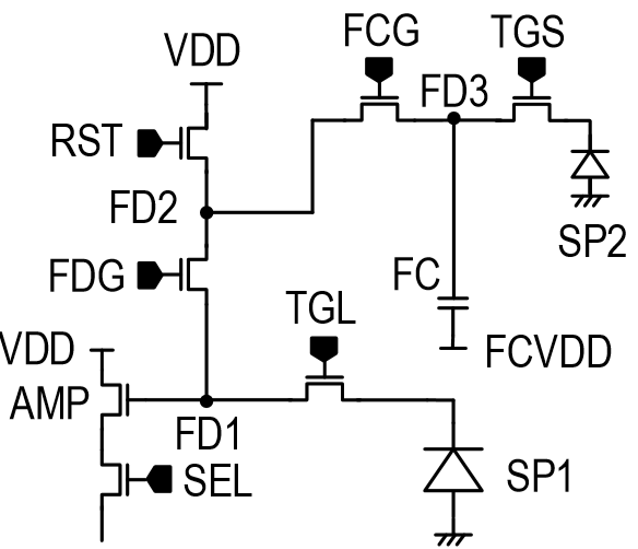
Sony presented a paper “A 132 dB single exposure dynamic range CMOS image sensor with high temperature tolerance”. This paper is an extension of the one presented at IEDM 2018. This pixel of IEDM 2018 is composed out of two photodiodes (small one for highlights, big one for lowlights). At the IEDM 2018 version, they were making use of three different sensitivity levels to create the high dynamic range. In the ISSCC2020 version, an extra sensitivity level is added to create a high dynamic range by means of four different sensitivity levels. So in total two photodiodes, the large one has two conversion gains, the small one has a single conversion gain, with the capability of overflow to an in-pixel capacitor. To operate the device in low noise, 8 readout cycles per pixel are needed, because for every signal (low/high conversion gain, small/large photodiode) also a reference signal readout is needed. The area ratio between the two photodiodes is reported to be 14.5, in the 2018 version, this ratio was 10.
The pixel structure is shown in the following figure (FC is the newly added capacitor) :
Some numbers :
- Pixel pitch : 3.0 um,
- FE 90 nm, BE 65 nm (1P4Cu), logic part :40 nm (1P6CU,1AL),
- Highest full well : 165,800 electrons, (this high full well is reached thanks to a vertical transfer gate instead of the classical planar one).
- Random noise 0.6 electrons,
- Single exposure (multiple reads) dynamic range : 132 dB.
The device is fabricated in a stacked technology, connection between the top and bottom layer is done on column level (TSV ?)
The title also refers to a high temperature tolerance, but in the presentation nothing was mentioned what has being done to obtain this high temperature tolerance, neither what was the gain in temperature tolerance w.r.t. other devices.
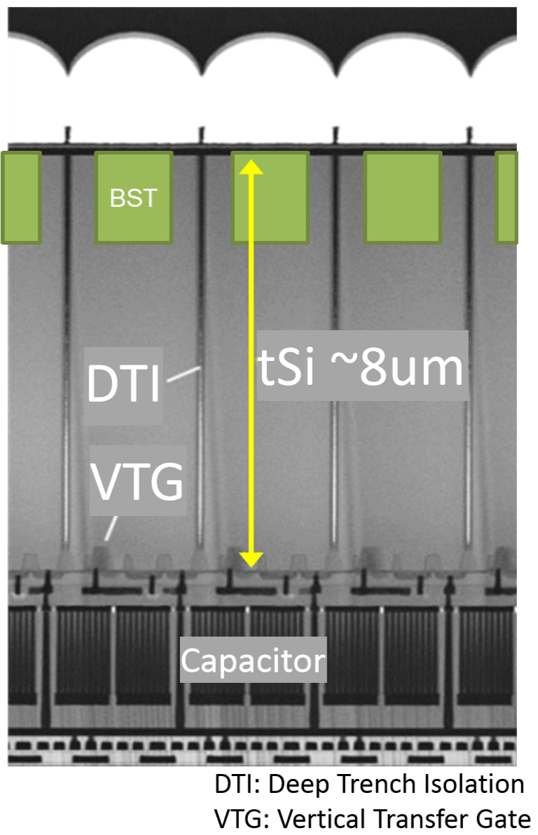
A global shutter paper was presented by Samsung : “A 2.1 e temporal noise and -105 dB parasitic light sensitivity backside-illuminated 2.3 um pixel voltage domain global shutter CMOS image sensor using high-capacity DRAM capacitor technology”. These days the titles of these talks are so long that actually all ingredients of the talk are already included in the title.
The paper is concentrating on the voltage domain global shutter option with correlated double sampling in the pixel. The authors referred to the issues with parasitic light sensitivity of the storage node in a charge domain global shutter and to the issues with kTC noise in the voltage domain global shutters if the storage capacitors are too small. The latter is solved in this paper by incorporating a high-capacity DRAM storage capacitor on top of the pixel. Because the technology is BSI, “plenty” of room is available to build an extra capacitor at the front-side of the pixel. This capacitor is not a stacked one, it is realized during the CMOS fabrication on top of pixel, in the third dimension.
The pixel itself has a classical structure that is known for voltage domain global shutter pixels, but a few extras are added : an extra transistor between the floating diffusion and the reset transistor to create a dual conversion gain, a clamping transistor to perform in-pixel CDS (based on clamping) and an extra capacitor that allows to short-circuit the in-pixel CDS and storage node, and actually allows the pixel to operate in the rolling shutter mode.
The device realizes the following performance :
- Pixel size 2.3 um,
- Stacked BSI (but the DRAM capacitor is not stacked !)
- Saturation level 12000 e– at low gain
- PLS : -115 dB (green)
- Performance at 940 nm : PLS = -95 dB, QE = 42 %,
- Read noise : 2.1 e– for 18 dB of gain,
- Frame rate : 120 fps.
The heart of this pixel is of course the DRAM capacitor on top of the front side of the pixel, a cross section is shown below :
(more to follow)
Albert, 19 February 2020.
I have a question about the sony split pixel:Why the FWC of SP2H is different from the FWC of SP2L? It seems that the charge is the same for SP2H and SP2L.
Because the capacitance, during readout, that is added to SP2H in comparison to the capacitance that is added to SP2L is different.
For SP2H it is the capacitance of FD3 that is added, for SP2L it is the capacitance of FD3 in parallel to FD2 in parallel to FCG that is added. So in the case of SP2L the capacitance is larger than in the case of SP2H.
Hopefully this is clear to you.
Best regards,
Albert.
Hello Albert,
For their new global shutter, Samsung reports 8.3msec of ‘read-out’ time.
Do they also state officially 120fps during the conference ?
120fps means 8.3msec per frame, including the full pixel timing or strictly the read-out?
Does this 8.3msec include the delay needed to charge the ‘huge’ 2×0.72pF/pixel capacitors ?
Would this impact the minimum integration time?
Best Regards,
Hi, I do not know the answer to your question.
If you want I can send you a pdf of the paper + a pdf of the presentation.
Just drop me a mail. Regards, Albert.
Hi albert
could you share me the pdf of the presentation about the Samsung global shutter?
Best Regards,
Hi, you can find it on the IEEE Explore website : https://ieeexplore.ieee.org/Xplore/home.jsp
Success, Albert.