Although most imaging engineers are aware about both technologies of butting and stitching, still some question marks exist about what is what ? This blog as well as the next one try to give some answers to this question.
Butting is referring to tiling closely together separate pieces of silicon to come to one large sensitive array. In principle all separate pieces of silicon can be operated as a single image sensor. In most cases butting is used to make imagers that are larger than the largest imager a single wafer can hold.
Stitching is referring to putting various design blocks together during the processing of the silicon, to make one large, stand-alone imaging array. All separate blocks of the design cannot be operated as a single image sensor, neither are they available as isolated dies. In most cases stitching is used to make imagers that are larger than the field of view of the lithographic equipment used during the fabrication of the imagers.
Are all buttable devices also stitched ? Most of them are, because in many cases stitching is needed to make the largest array possible on a single wafer. If that imager is still not large enough, butting is the only solution.
Are all stitched devices also buttable ? For sure not, because not all stitched devices have a wafer-level size.
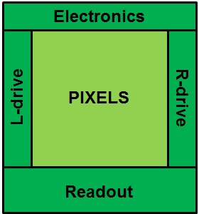
In Figure 1 a simple sketch is shown of an imaging array : the pixel matrix is surrounded by a left-driving and right driving circuitry, a readout part at the bottom and some extra electronic circuitry at the top.

Figure 1 : Sketch of the floor plan of an image sensor.
This sensor is not designed to be butted, because the circuitry around the imaging matrix is preventing a contiguous larger imaging area when two or more devices are placed next to each other. To make this device buttable, at the circuitry along at least one side needs to be removed in the design. An example is shown in Figure 2, with the result after butting in Figure 3.

Figure 2 : One-side buttable imaging array.

Figure 3 : Two devices butted together based on the device concept of Figure 2.
As can be seen in Figure 3, the total light sensitive array is twice as large as the size of a single device. Butting will never ever be perfect in the sense that there will always some pixels missing between the two pieces of silicon. But in most applications, the number of lines (in Figure 3) of missing pixels is limited to a single line of pixels. It has to be mentioned that devices that are butted normally do not use small pixels. But pixel sizes of several tens of micro-meters are very common for buttable devices.
The limitation of the sketch in Figure 3 is clear : only a factor of 2 ins ensitive area can be gained by butting 2 devices. If a larger sensitive area is needed, buttability needs to be possible along more than 1 side, for instance 2 sides, as shown in Figure 4.

Figure 4 : Two-sides buttable imaging array.

Figure 5 : Four devices butted together based on the device concept of Figure 4.
The same accuracy as mentioned before can be obtained along the butting lines : only one column or one row of pixels will be missing. Notice the rotated arrangement of the dies in Figure 5. From bottom left to bottom right, rows are becoming columns and columns are becoming rows, etc. So a little extra data reshuffling is needed after readout, but after all, a factor of 4 can be gained in light sensitive area compared to a single die shown in Figure 4.
A buttable configuration with more flexibility can be found with devices that are 3-sides buttable, shown in Figure 6.

Figure 6 : Three-sides buttable imaging array.
All electronics needed to drive the sensor is no longer available at the sides, neither at the top of the chip. But the drivers and timing circuitry is placed between the pixels themselves. The lay-out of the chip is becoming more and more sophisticated, because as can be seen in Figure 7, butting does not allow any circuitry at the butting edges.

Figure 7 : Six devices butted together based on the device concept of Figure 6.
But the big advantage of this design is the unlimited butting capability in one direction. Of course in the other direction the number of devices is limited to 2.
The latter architecture is widely used for medical (mainly CMOS) and astronomy (mainly CCD, slow shift towards CMOS) applications. With today’s 300 mm wafer sizes, single monolithic sensors of 200 mm x 200 mm on a single wafer can be made. And with the butting x mm (H) x 400 mm (V) are possible, where x is defined by the application and the cost of the assembled device. (With a rectangular footprint of the sensor instead of a square one, even larger butted imaging arrays are possible.)
What about 4 sides buttable ? To my knowledge a 4-sides buttable device is never realized in CMOS technology, although there were some attempts in the past to build 4-sides buttable CCDs. But the wiring and the connections to the outside world are becoming extremely complex and difficult. And with the existence of 300 mm wafers, there is much less justification left to design and fabricate 4-sides buttable devices (maybe with the exception of astronomy applications).
Next time the focus will be on stitching,
Albert, 17-06-2016