Archive for February, 2016

Imaging Trainings scheduled for Spring 2016

Saturday, February 27th, 2016

Maybe it is good to remind the visitors of this blog about imaging trainings in the Spring 2016.  There are 6 courses in the pipeline :

– a 2-day class to get an introduction in the world of CMOS image sensors.  This class is intended for people who have almost no background in solid-state imaging.  This course takes place in Taufkirchen (Munich) on June 29-30, 2016, organization through www.framos.com.

– a 5-day class if you want to learn more about imagers than just the working principles.  Also this class is intended for “new-comers” in the field, but also people working already a few years in imaging can revitalize their knowledge.  The course can be considered as the mother of all trainings offered by Harvest Imaging.  Key to this class are the exercise sessions at the end of every day helping the participants to put the theory into practice.   This course takes place on April 4-8, 2016 in Barcelona, and is organized by www.cei.se.

– a 2-day class with hands-on measurements and evaluation of an “unknown” camera.  Because the participants have to perform all characterization work themselves, this course is NOT intended for people fresh in the imaging field.  Preferably the course participants have a few years of experience in the arena of solid-state imaging.  This course takes place in Munich, on March 30-31, 2016, organized by www.framos.com, as well as in Amersfoort, on May 26-27, 2016, organized by www.cei.se.

– a 3-day advanced class focusing on CMOS image sensors.  Because the material presented is on a higher level, this course is intended for people who have a couple of years of experience in the field of digital imaging.  The course is scheduled for May 23-25, 2016 in Amersfoort (Nl), organized by www.cei.se.

– a 3-day course on Digital Camera Systems.  In this training the focus is less on the image sensors, but more on the processing of the signal delivered by the image sensor.   The complete colour processing pipe will be explained and demonstrated by an extensive amount of images and algorithms.  The participants will get a soft copy of all images shown in the course.  Location will be Barcelona, date : June 14-16, organized by www.cei.se.

Looking forward to see you at one of these courses.

Albert, 27 February 2016
Noise Forum at ISSCC 2016

Monday, February 8th, 2016

The ISSCC forum, organized on Thursday, was focusing on Noise in Sensors (very general).  A total of 9 presentations were given, of which (only) 3 focused on Imagers.  The undersigned opened the forum with a general overview of Noise in Image Sensors, in the early afternoon Shoji Kawahito give a presentation on Low-Noise Image Sensors, and to conclude the forum, Neale Dutton had a talk about Noise in Single-Photon Detectors. 

On one hand many people appreciated the general overview of noise present in many different type of sensors, on the other hand, not that many imaging engineers attended the forum because of the low number of talks about imagers.  Nevertheless, the ISSCC organization seemed to be pretty happy with the number of registrations. 

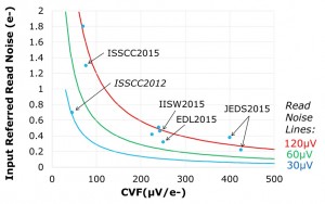
One very interesting detail from Neale’s presentation : he showed a very nice graph of published noise data which I include here in this blog (with permission of Neale !).  On the vertical axis the input referred read noise in electrons is shown versus the conversion gain of the pixels.

The three lines shown in the graph are lines of equal read noise, “equinoise” lines, but this time noise expressed in uV.  As can be seen, the lowest noise ever reported was 0.22 electrons, presented in JEDS2015, but the lowest noise ever reported in the voltage domain was 30 uV, presented at ISSCC2012.  I do know that expressing noise in equivalent number of electrons is a very common technique which I support as well, but nevertheless, looking to the noise in the good, old classical way gives a complete other image.  Now the challenge is to keep the 30 uV of noise level alive, while increasing the conversion gain !

Thanks Neale (not Neil) for this “fresh” view on the noise !

Albert, 08-02-2016.

ISSCC 2016 (3)

Monday, February 8th, 2016

In this third and last review of the ISSCC, 2 remaining imaging papers are left.

The first one comes from NHK, and deals with a 1.1 um 33 Mpixel device, 3D stacked and 3-stage cyclic-based ADC.  This 3D stacking is realized by means of direct bonding (in the columns).  TSV’s are avoided because they seem to be too expensive, they cost more masks, they consume area and they make a more complicated lay-out needed.  The device is fabricated at TSMC (at least TSMC is mentioned in the acknowledgement), and to my knowledge this is the first CMOS image sensor made in 45 nm 1P4M.  The logic part on the second level of silicon is made in 65 nm 1P5M technology.

The ADC implemented on the chip (by Shizuoka Univ./Brookman Technology) is a three stage design, the first two stages are cyclic ADCs (upper 3 bits and middle 6 bits), the last stage is  a SAR ADC (3 bits).  The sensor can run at full resolution (33 Mpixels !) at a rate of 240 fps, burning 3 Watts.

The last paper from the imaging session is the one that was published by FBK, Trento, with two brothers as authors (does not happen that often).  The device presented is intended for spacecraft navigation and landing.  It contains 64 x 64 pixel digital silicon photomultiplier direct ToF with 100 Mphotons/s/pixel background rejection.  Every pixel (out of the 64 x 64 array) contains 8 SPADs  with extra electronic circuitry.  The pixel is designed such that uncorrelated photons or dark current (which still trigger the SPADs) do not give an output from the pixel.  Only correlated photons give an output.  So the background suppression and dark count suppression is more or less based on the statistics of these signals (compared to the ToF signal), and is implemented in the digital logic within every pixel.  Fabrication technology is 150 nm CMOS with 6 metal layers.  Pixel fill-factor is 26.5 %.

Albert, 08-02-2016.

ISSCC 2016 (2)

Friday, February 5th, 2016

At ISSCC several high resolution imagers were presented.  Champion was the device of CMOSIS with 391 Mpixel device for airborne mapping applications.  The device itself is pretty straight forward with 3.9 um pixel pitch, 4T non shared pixels, 31.5 ke full well, 45 uV/e conversion gain, 3.7 e of noise at unity gain, resulting in 78 dB dynamic range.  The 14-bit SS ADCs are placed in the columns and are located at the two sides of the imager.  So the pitch of the ADCs is 7.8 um.  Jan Bogaerts showed impressive images of the device, and after the “show” I had the opportunity to take a look at a real device in its package.  The sensor is using stitching : 6 x 3 blocks are stitched in the active area, with 4352 x 5000  pixels in each stitched block.  Processing was done at ST in a 90 nm FE/65 nm BE process 1P4M.  The device is monochrome, but in the final application, this monochrome sensor is surrounded by CCDs that provide the colour information.  During Q&A it was mentioned that the camera is using a mechanical forward motion compensation technique to compensate for the movement of the camera during exposure.

During the presentation Jan Bogaerts made a comparison with a CCD of the competition.  Amongst several characteristics, he mentioned that his CMOS sensor is free of smear in contradiction to the CCD.  In a private discussion afterwards with Jan Bogaerts he told me that the camera is using a mechanical shutter (that is no secret I guess), but one should realize that in that case a CCD is neither showing any smear issues.

Hirofumi Totsuka of Canon presented a 250 Mpixel APS-H size imager : 1.5 um pixel pitch (4 sharing) made in 0.13 um technology node.   The device is consuming 1.97 W at full resolution 5fps.  An interesting build-in feature of this sensor is the following :  ALL pixel signals are converted by column SS-ADCs with a single ramp, but in front of the ADC, each column has its own PGA that can be switched to 4x or 1x gain, depending on the signal level.  So when the pixels are sampled, a first check is done to look whether the signal is above or below a particular reference level, and then the right gain of the PGA is set to 1x or 4x.  Simple method, but I think that the issues pop up in the reconstruction of the signal at the cross-over point between the two settings of the PGA.


Kei Shiraishi of Toshiba presented a stacked sensor with 1.2 e of noise with a comparator-based multiple sampling PGA.  The most important characteristic is the multiple sampling in the analog domain.  This goes much faster than the multiple sampling in the digital domain.  After 32 samples of each signal, a noise level of 1.2 e could be reached for 1 M pixels at 20 fps.  The device is realized in 65 nm, both for the sensor as well as for the circuit on the second silicon level.  It was mentioned in the paper, but I guess that the noise floor without the multiple sampling should be around 5 e at 30 fps, going down to the 1.2 e reported at 20 fps.

Charles Liu of TSMC showed the results obtained by a 33 Mpixel, stacked device with a negative substrate bias.  The idea is actually pretty simple, maybe the implementation is more complicated. “Simply” bias the substrate of the sensor to -1.3 V and you can lower all other supply voltages by 1.3 V.  So instead of having a power supply of 3.3 V, the device has now a supply of 2.0 V.  But the large pixel swing is maintained by means of the negative substrate bias.  The sensor is fabricated in 65 nm 1P5M technology.

Albert, 05-02-2016.

ISSCC 2016 (1)

Thursday, February 4th, 2016

Already quite a bit of words are spent on the organic conductive sensors presented in the Panasonic papers.  Nevertheless, here is some more info.

Kazuko Nishimura presented the paper on the large HDR sensor with a low noise level.  A few remarks about this sensor :

–          HDR is obtained by two light sensitive areas within one pixel : one with low and one with high sensitivity.  This is a very similar method as proposed long time ago by Fuji in their SuperCCD,

–          The pixels do suffer from kTC noise, but by means of a cleaver circuit/feedback, they are able to reduce the remaining kTC noise to 1.2 e reset noise and to 5.4 e overall.  In combination with a full well of 600 ke, it creates a gorgeous dynamic range,

–          The process used to fabricate the sensor is 65 nm CMOS, 1P3Cu1Al,

–          The results mentioned are overall not bad, but there was no information provided about dark current, about quantum efficiency, about uniformity and about reliability of the material.  So this suggests (to me) that there are still some issues to solve.

Sanshiro Shishido presented the paper on the global shutter version of the organic photoconductor sensor.  The topplate of the photoconductor is made out of ITO and needs to be biased to larger voltages.  But the overall light sensitivity of the organic photoconductor depends strongly on the exact voltage on the ITO gate.  A lower voltage on the ITO gate lowers the light sensitivity and actually 0 V on the gate makes the sensor even blind.  In this way one can create a global shutter functionality to the sensor.  Moreover, one has the possibility to modulate the sensitivity during the exposure time, for instance, the exposure time can be split in parts in which the sensor will be sensitive and in parts in which the sensor will be insensitive.  Even one has the option to modulate the sensitivity during the periods the sensor is sensitive by means of adapting the high voltage set to the ITO gate.  Overall a nice technology !

The third paper of Panasonic, presented by Yoshihisa Kato had nothing to do with the organic conductive layer, but the sensor presented was provided with an EM-function.  The latter is built in the vertical direction of the silicon.  This is new and is never shown before in an imager (to my knowledge).  The EM-functionality can be switched on and off by means of the voltage biasing the substrate (around 23 V).  Amazing images were shown (shot at extremely low light levels).  From the data shown, it looks like the EM is very strongly depending on the exact voltage on the substrate.  In comparison to the well-known EM-CCD and EM-CMOS devices (which are on the market), the EM-multiplication in the latter is done with very small gain steps, but by doing multiple EM-steps finally a large gain can be reached.  In the case of the Panasonic paper, the EM is done only once, so all the gain needs to be created in one step.  Has this way of working advantages or disadvantages compared to EM-CCD and EM-CMOS ?

Albert, 04-02-2016.