Merry Christmas and Happy New Year

December 20th, 2013

Good Bye 2013 !  The year is almost over.  And as I did in the foregoing years, also this time I would like to take a quick look back and see what 2013 brought to us.  Also now I can repeat that the year 2013 was again a great year for Harvest Imaging !  The year started with the move towards a new office space.  In the meantime all furniture, equipment and infrastructure is installed and in operation.  So most of the blogs you could read this year were “born” from my new office space.  This is especially true for the blogs that contained measurement data.

If I overlook the “products” of Harvest Imaging, I can split them up into three groups :

  • The training courses, in-house as well as public courses.  It is and remains amazing and sometimes hard to believe where all the people are coming from that attend the courses.  In 2013 I had a training almost every other week, and I just completed course number 150 !  It is very motivating to experience that so many young engineers step into the challenging but very rewarding world of imaging,
  • The consulting activities.  I hope that my readers do understand that I cannot elaborate on this because of confidentiality reasons.  But I can indicate that my expertise was used in the field of imaging technology as well as intellectual property related projects,
  • The new product of Harvest Imaging, being the organization of the Solid-State Imaging Forum.  The very first edition of this forum was organized this December, focusing on “ADCs for Imagers”.  It was really a success and the large attendance proofs that there is a need for this kind of in-depth information and knowledge exchange.

To conclude this overview of products, it is a pleasure for me to thank all my customers who brought business to Harvest Imaging, in one way or another.  It is great to experience your trust and confidence by consulting the expertise of Harvest Imaging.  Thanks very much !

2013 is an odd number, and it inherently translates into another International Image Sensor Workshop, this time in the USA.  My friends in the field, Boyd Fowler, Eric Fossum and Gennadyi Agranov, organized another great Workshop.  Location was Snow Bird in Utah, where all technical information was exchanged, distributed and absorbed (literally) at a very high level.  Although again the technical and scientific level of the Workshop was outstanding, the highlight for me was the “meet and greet” with Michael Tompsett, the real inventor of the CCD image sensor.  He gave a very impressive overview of his history in the CCD imaging world and clearly explained to the audience that the 2009 Nobel Prize for the invention of the CCD image sensor went to the wrong person.  Thanks to the chairs of the Workshop to take the initiative to invite Michael Tompsett !

To conclude, I wish all of you the very best for 2014, and hope that we will regularly “meet” through this blog.  Thanks for visiting the website of Harvest Imaging, hopefully see you next year.  Welcome 2014 !

Albert, 20-12-2013.


How to Measure Full Well Capacity (3)

December 6th, 2013

From the two foregoing discussions on the full well capacity, it could be learned that :

–       In the case the full well is determined/limited by the ADC, comparable results for the FWC can be obtained by means of linearity measurements as well as from the mean-variance method,

–       In the case the full well is not determined/limited by the ADC, the results obtained from the linearity measurements show larger full well values than the ones obtained from the mean-variance method.

To explain the discrepancy between the FWC data of the latter case, one should realize that when the average output signal turns into saturation, a few non-uniformity issues are simultaneously popping up :

–       PRNU or photo-response non-uniformities : the pixels with the highest sensitivity can reach saturation first,

–       Non-uniformities in saturation level, some pixels will saturate at a lower FWC than others,

–       It is not clear from the measurements which part of the pixel is causing the saturation : the pinned-photodiode, the floating diffusion capacitance, the output swing limitation of the source-follower, output limitation swing of the analog circuitry.  Moreover, all these limitations can interfere with each other, which makes the situation even more complex to understand and explain.

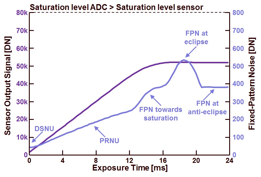
To find out what is going on, the fixed-pattern noise is measured, and some interesting results were obtained.  The analog gain is put to a low value, and the reference voltage of the ADC is set to a higher voltage (the reference voltage is defining the analog input voltage that corresponds to an output of all “1”s).  In this way the ADC is not limiting the output swing, neither defining the FWC.

The measurement results are shown in the figure 1 : the left axis indicates the average output signal of 100 x 100 pixels as a function of the integration/exposure time; the right axis shows the fixed-pattern noise obtained from these 100 x 100 pixels, also as a function of the exposure time.

Figure 1 : Average sensor output and fixed pattern noise as a function of exposure time for a window of 100 x 100 pixels.

Some interesting details can be revealed from the FPN data :

–       For very low values of the signal (exposure time < 1 ms), the FPN shows a kind of plateau, indicating the FPN in dark,

–       For moderate values of the signal (1 ms < exposure time <12 ms), the FPN linearly increases, determined to the PRNU, the latter is proportional to the average signal value,

–       For higher values of the signal, in the region where the output signal tends to saturate (12 ms < exposure time < 16 ms), the FPN grows faster and tends to saturate as well.  Most probably this is the effect of the pixels that saturate.  The FPN at saturation is larger than the PRNU and for that reason the FPN increases.  The FPN tends to saturate, because once all pixels are saturated, the FPN does no longer change,

–       For saturated values of the signal (16 ms < exposure time < 20 ms) the FPN gets a second boost.  It is not completely clear what is happening here (the camera and sensor are “unknown”), but most likely the double sampling of the reference and useful signal start showing some “black sun” or “eclipse” effects.  This results in a larger FPN,

–       For the largest exposure times (exposure time > 16 ms), all pixels are running in the “black sun” or “eclipse” mode, but apparently the sensor is provided with an anti-eclipse circuit which pins the column voltages to a fixed voltages.

The abovementioned explanation is based on a close observation of what the behavior of the output signal.  This is illustrated in Figure 2, showing the same results as the ones mentioned in Figure 1, but with an adapted scale on the vertical axis.

Figure 2 : Same data as shown in Figure 1, but with an adapted scale on the left vertical axis.

As can be noticed, the average output signal tends to reach saturation for an exposure time of (about) 17 ms, but then the average output signal decreases again for a longer exposure time.  From 20 ms onwards, the average output signal seems to be clipped to a particular value, so does the FPN.  A simple explanation for this effect can be the presence of an anti-eclipse circuit.

Anyone else has a better explanation ?

Albert, 06-12-2013.

Forum ADC’s for Imagers is completely SOLD OUT !

December 4th, 2013

The two planned sessions on Dec. 16-17, and Dec. 19-20, 2013 are completely sold out.  There is no need for further regsitration because more seats will not be added.  Thanks to all people who registered.  I will keep you updated about the feedback of the participants.  At that time I will also start with the preparation of a new forum in 2014.

Albert, 4-12-2013.

Status Imaging Forum “ADCs for Imagers”

November 15th, 2013

I just want to give the imaging community a quick update on the registration situation for the forum “ADC’s for Imagers”.

Because the interest was/is much higher than expected, a second session will be organized (this was already announced earlier), and the number of seats is each session is slightly increased (from 24 to 32).

At this moment registration for the forum is still possible, because :

– for the session on Dec. 16 & 17, 2013, there are still 2 seats left,

– for the session on Dec. 19 & 20, 2013, there are still 3 seats left.

If anyone is still interested for registering, take your chance !  Keep in mind that in 2014 the forum will be organized again, but with a different subject !


Albert, 15-11-2013.

How to Measure Full Well Capacity (2)

November 4th, 2013

In the previous blog, the measurement of the full well capacity (FWC) was explained based on the measurement of the output signal versus the input signal.  The input signal was generated by a constant light source in combination with a varying exposure time.  But once all output data is available, not only the average value of the pixels can be calculated but also the temporal noise level for every pixel.  This will be done in this blog.

From the discussion of the photon-transfer curve and its properties, it was learned that when the photon shot noise is the dominant noise source, the following formula can be written down :

ntemp2 = k×(Sout – Soff)

with :

ntemp : the total temporal noise on pixel level,

k : conversion gain,

Sout : the average signal on pixel level,

Soff : offset value, or the average signal for 0 s exposure time.

(Normally I use a sigma-symbol for the noise, but the bloody software does not accept the sigma-symbol.)

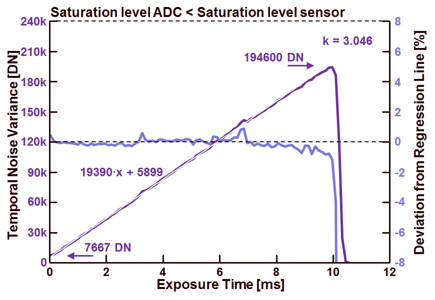
So instead of looking after the saturation level of the signal, one can also look after the saturation or the peak level in noise and try to calculate the FWC based on the noise measurements.  The FWC is defined at the point at which the temporal noise reaches its maximum value.

1)    Saturation of the sensor is larger than maximum value of the ADC.

In such a case, most of the time the maximum value of the sensor or camera ADC is set such that the complete ADC range covers the linear part of the sensor’s output response.  An example of a camera in which the ADC defines the maximum output level of the system is shown in Figure 1, where the sensor noise variance is shown as a function of the exposure time (the data already collected in the previous blog is reused here).

Figure 1 : Noise variance as a function of exposure time, under a constant illumination level.

Shown is the temporal noise variance as a function of the exposure time at a constant illumination level (the exact value of the light input is not important for this measurement, as long as it stays constant).  As can be observed, the transition from a monotonically increasing output value of the variance to zero goes pretty abruptly.  This is a clear indication that the ADC defines the saturation level.  Moreover, the peak value of the temporal noise variance is equal to 194,600 DN.

For this example, the definition of the full well capacity is equal to the variance peak value divided by k, minus the offset  value of the noise variance at 0 s exposure time divided by k, or (194,600/k) – (7667/k) = 63,887 – 2517 = 61,370 DN.

Taking into account the conversion gain of the sensor (3.046 DN/electron, for the TIFF format it is 64x larger than what can be measured at the output of the sensor), this results in a FWC = 20,148 electrons.

2)    Saturation of the sensor is smaller than maximum value of the ADC.

In this case, the FWC needs a clear definition : is FWC referring to the saturation level of the sensor/camera, or is FWC referring to the maximum linear part of the sensor’s output swing ?  The former can be referred to a FWCsat, while the latter can be indicated by FWClin.  But now the question arises : how to define the linear part of the sensor’s output swing ?  In the previous blog, FWClin was set at the point where the sensor’s output deviated maximum 3 % of the linear behavior.  Taking that definition and transferring it to the noise variance measurement, now FWClin will be defined at the point where the noise variance deviates maximum k×(3 %) = 4.5 %.

An example of a camera in which the ADC maximum output value is larger than the saturation level of the sensor is shown in Figure 2.

Figure 2 : Noise variance as a function of exposure time, under a constant illumination level.


Shown is the temporal noise variance as a function of the exposure time with a constant illumination level (the exact value of the light input is not important for this measurement, as long as it stays constant).  As can be observed, the transition from a monotonically increasing output value to a decrease of the noise variance goes smoothly.  This is a clear indication that the ADC is NOT defining the saturation level of the system.

For this example, the definition of the full well capacity at saturation is equal to the maximum level of the noise variance divided by k, minus the offset of the noise variance measured at 0 s exposure time and also divided by k, or (41,260/k) – (2389/k) = 27,013 DN.  Taking into account the conversion gain of the sensor (1.493 DN/electron), this results in a FWCsat = 18,093 electrons.


But as mentioned before, this is only half of the story, because the sensor’s response is very nonlinear close to saturation.  For that reason the linearity (INL) of the sensor is characterized and plotted in Figure 2 as well.  At the point where the real output characteristic deviates 4.5 % from its regression line, the FWClin is defined.  In this example, the following number can be found : (39,780/k) – (2389/k) = 25,044 DN, translating in FWClin = 16,774 electrons.

It should be clear that this last number is very much depending on the definition of FWClin.  If the 4.5 % deviation is translated in 1.5 %, the value for the FWClin will become smaller, or if the 4.5 % deviation is translated in 7.5 %, the opposite becomes valid.


Note : the data shown in Figures 1 and 2 are obtained from the same sensor, with the same light input.  The difference between the two measurements is a difference in camera setting, such that the analog gain of the sensor and the reference voltage of the ADC result in an overall camera gain difference of a factor of 2.

Explained in this blog is the measurement of FWC based on noise variance.  Again it can be learned that the values obtained for the FWC strongly depend on the exact definition of the full well capacity.  Lesson to take away : if the FWC is specified in an image sensor’s datasheet, first ask yourself “How is the FWC defined ?”.

See you next time !

Albert, 04-11-2013.

Post-Doc Opening at TU Delft

October 13th, 2013

On a very short notice, I will start with a couple of new projects at the TU Delft.  The main emphasis of the projects will be ultra-low noise CMOS image sensors.  A post-doc position is open for a project leader for these projects.  Preferably, the candidate for this position has a background (=PhD degree) in solid-state image sensing and/or mixed signal-design.  Those who might be interested can directly contact me : a.j.p.theuwissen at tudelft.nl, and it would be very helpful if you can send me your resume right away.

Albert, 13-10-2013.

How to Measure Full Well Capacity (1)

September 27th, 2013

The next parameter to be characterized is the full well capacity of the sensor.  But before any measurement or characterization can be done it is important to make clear what is the definition of the full well capacity (FWC).  To come to that point, let’s treat two different situations, the first one in which the ADC is setting the saturation of the sensor and the second one in which the ADC is not setting the saturation of the sensor.

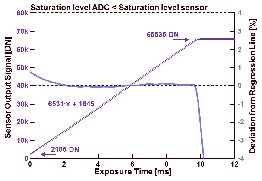
1)    Saturation of the sensor is larger than maximum value of the ADC.  In such a case, most of time the camera/sensor designer is setting the maximum value of the ADC such that the complete ADC range covers the linear part of the sensor’s output response.  An example of a camera in which the ADC defines the maximum output level of the system is shown in Figure 1.


Figure 1 : Sensor output value as a function of exposure time, under a constant illumination level.

Shown is the sensor output as a function of the exposure time with a constant illumination level (at this stage of the discussion, the exact value of the light input is not important for this measurement, as long as it stays constant, so that various setting of the camera and/or sensor can be compared with each other).  On the right axis the integral non-linearity is shown as well.  As can be observed, the transition from a monotonically increasing output value to saturation goes pretty abruptly.  This is a clear indication that the ADC defines the saturation level.  Moreover, the value of the saturated output is equal to 216 – 1 = 65535 DN (216 is coming from the TIFF format).

For this example, the definition of the full well capacity is equal to the saturation level (of the ADC) minus the offset at zero seconds exposure time, or 65535 – 2106 = 63429 DN.  Taking into account the conversion gain of the sensor (3 DN/electron, for the TIFF format it is 64x larger than what can be measured at the output of the sensor), this results in a FWC = 19820 electrons.

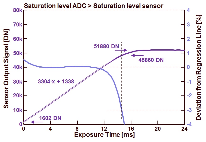
2)    Saturation of the sensor is smaller than maximum value of the ADC.  In this case, the FWC needs a clear definition : is FWC referring to the saturation level of the sensor/camera, or is FWC referring to the maximum linear part of the sensor’s output swing ?  The former can be referred to a FWCsat, while the latter can be indicated by FWClin.  But then the question arises : how to define the linear part of the sensor’s output swing ?  Very often, FWClin is defined at the point where the deviation of the sensor’s output and an ideal straight line is maximum 3 %, or at the point where the sensor’s output is linear up to 97 % or better.  An example of a camera in which the ADC maximum output value is larger than the saturation level of the sensor is shown in Figure 2.

Figure 2 : Sensor output value as a function of exposure time, under a constant illumination level.


Shown on the left vertical axis is the sensor output as a function of the exposure time with a constant illumination level (the exact value of the light input is not important for this measurement, as long as it stays constant), shown on the right vertical axis is the corresponding integral non-linearity (INL).  As can be observed, the transition from a monotonically increasing output value to saturation goes smoothly.  This is a clear indication that the ADC is NOT defining the saturation level of the system.

For this example, the definition of the full well capacity at saturation is equal to the saturation level minus the offset at zero seconds exposure time, or 51880 – 1602 = 50278 DN.  Taking into account the conversion gain of the sensor (1.5 DN/electron), this results in a FWCsat = 33518 electrons.

But as mentioned before, this is only half of the story, because the sensor’s response is very nonlinear close to saturation.  For that reason the linearity (INL) of the sensor is characterized and plotted in Figure 2 as well.  At the point where the real output characteristic deviates 3 % from its regression line, the FWClin is defined.  In this example, the following number can be found : 45860 – 1602 = 44258 DN, translating in FWClin = 29505 electrons.

It should be clear that this last number is very much depending on the definition of FWClin.  If the 3 % deviation is shifted to 1 %, the value for the FWClin will become smaller, or if the 3 % deviation is shifted to 5 %, the opposite becomes valid.


Note : the data shown in Figures 1 and 2 are obtained from the same sensor, with the same light input.  The difference between the two measurements is a difference in camera setting, such that the analog gain of the sensor and the reference voltage of the ADC result in an overall camera gain difference of a factor of 2.

Explained in this blog is the measurement of FWC based on linearity measurements.  Again it can be learned that the values obtained for the FWC strongly depend on the exact definition of the full well capacity.  Lesson to take away : if the FWC is specified in an image sensor’s datasheet, first ask yourself “How is the FWC defined ?”.

See you next time !

Albert, 27-09-2013.

Playing Time (3)

September 9th, 2013

Once more thanks for all the reactions.

I checked the reactions again this morning, and it is clear that the right answer/suggestion came from David San Segundo Bello (imec).  Already in one of the very first reactions, he mentioned a possible drift of the LED light source due to an AC variation on top of the DC voltage.  Afterwards Guy Meynants (CMOSIS) repeated the answer of David, but also added to it the method to check it out, namely by means of noise measurements.  That actually completed the story.  So I think it is fair to give both guys a bottle of wine.

Albert, 09-09-2013.

Playing Time (2)

September 6th, 2013

It was surprising to see the amount of reactions on the previous “Playing Time” blog.  Thanks for all the remarks, questions, suggestions, also through the www.image-sensors-world.blogspot.com web-site.

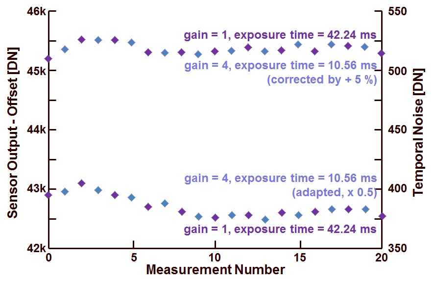
Remember what the issue was : measurements were done with a constant LED light input at two different settings :

–       gain = 1, exposure time = 42.24 ms, 100 images, and,

–       gain = 4, exposure time = 10.56 ms, 100 images.

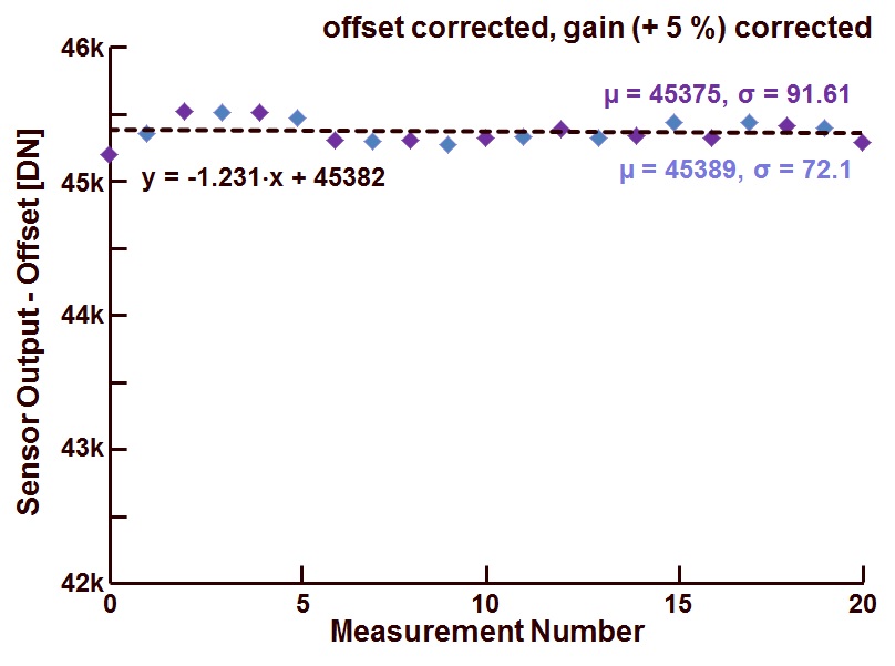
A constant switch between the two settings was realized, and in total 21 (times 100 images) measurements were done to check the reproducibility.  Based on the numbers shown, one would expect the same output in all situations.

A first issue, being the offset that does not scale with the gain, was corrected by subtracting the (measured seperately) offset for all measurements.  A second issue, being the incorrect ratio of gain setting (theory 1:4, reality 1:3.8) was corrected, and then the final result is shown in Figure 1.

Figure 1 : Sensor output values (corrected for the offset and corrected for incorrect gain setting) as a function of measurement number (each dot represents the average value of a 50×50 ROI of 100 images).

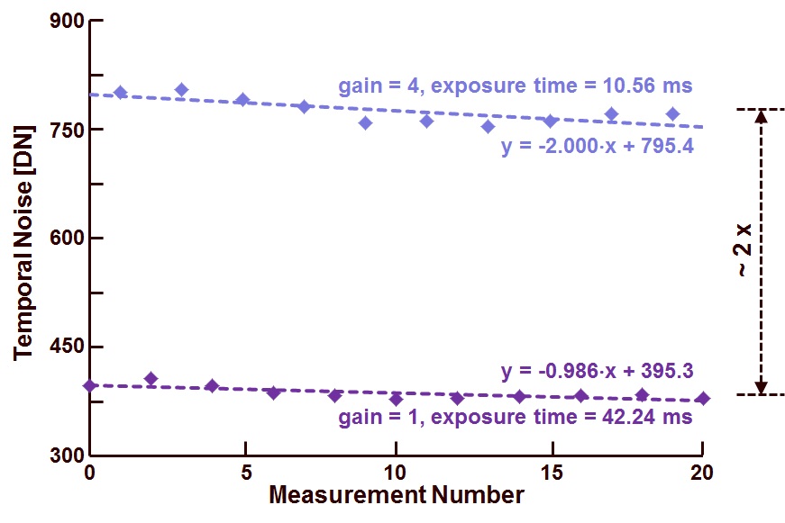
To find the root cause of the fluctuations fo the output signal, the temporal noise on pixel level is calculated, this excludes the FPN of the pixels.  The result of the measurement is shown in Figure 2.

Figure 2 : Noise calculations of the measurements performed in Figure 1 (each dot represents the average value noise value of a 50×50 ROI of 100 images).

Notice that, although the output signal in both cases is expected to be the same, that is not the case for the noise !  The temporal noise is dominated by photon shot noise and if the cases of “gain = 1” are set as the references, then the photon shot noise (expressed in electrons) for the cases of “gain = 4” is a factor of 2 less in the charge domain (4 times less photons).  But with a gain setting that is 4 times higher, the temporal noise in the digital domain becomes a factor of 4 higher.  Compared to the cases of “gain = 1”, the noise in the digital domain of the cases of “gain = 4” will be factor of 2 higher.  This is pretty much the case for the measurements (proving that the measurements and calculations were done right).

If the noise of the “gain = 4” cases is reduced by a factor of 2, and if then the noise results are plotted together with the output signals of the sensor, Figure 3 is generated.


Figure 3 : Measured output signal (corrected where needed) and calculated temporal noise (adapted where needed) of the measurements performed.

With a bit of imagination, a similar pattern that was present in the measurements of the output signal can be found in the calculated temporal noise.  There is enough correlation between both to conclude that the changes in the output signal was coming from the light source, because the fluctiations are reflected in the (photon) shot noise results as well.  (After some experiments, it was found that the power supply for the LEDs was causing the issues, because its output voltage was not stable over time.)

This exercise illustrates the power of using noise measurements as a diagnostic tool !

Albert, 06-09-2013.

Status Imaging Forum “ADCs for Imagers”

September 3rd, 2013

Due to the large interest for the first Imaging Forum “ADCs for Imagers”, two sessions are now scheduled : the first one on 16 & 17 Dec. 2013, the second one on 19 & 20 Dec. 2013.  Unfortunately a few people had to cancel their pre-registration, so a few seats (for both sessions) are back available for those who still are interested.  Please notice that a third session will not be organized.  In the year 2014, another forum will be planned, but with another subject !

Albert, 3-9-2013.