How to Measure : Fixed-Pattern Noise at Saturation

May 1st, 2012


There is one important fixed-pattern noise component left in the discussion about how to measure the FPN with or without light input, being the FPN at saturation.  These days most of the pixels have a built-in anti-blooming drain, e.g. lateral or vertical anti-blooming in CCDs or anti-blooming via the reset transistor in CMOS devices.  In all cases the anti-blooming characteristics of the pixels is relying on a “parasitic” transistor that opens at the moment that the pixel is going into saturation.  Because all these “parasitic” transistors differ in threshold voltage, all pixels have different anti-blooming characteristics, resulting in a (large) FPN component at saturation.  To measure this component of the FPN, the devices need to be driven into saturation, and the variation along the pixels can be characterized.  By itself, this is a very simple measurement.

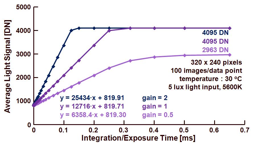
Figure 1 shows the output characteristics of an imager (= average output signal of all green pixels) as a function of the exposure or integration time.  The input settings are indicated in the figure.

120420_blog_1


Figure 1 : Average output signal of all green pixels as a function of the exposure time.

In Figure 1, three curves can be recognized, respectively for a setting of the on-chip analog amplifier equal to 2, 1 and 0.5.  As can be seen, the curves for a gain equal to 2 and 1 saturate at 4095 DN.  This indicates that the ADC is determining the saturation level of the signal and not the pixels themselves.  The situation is different for a gain equal to 0.5.  In that case the saturation level is within the range of the ADC, indicating that the sensor itself is saturating and not the ADC.  In this example, the saturation at a gain equal to 0.5, is 2963 DN.

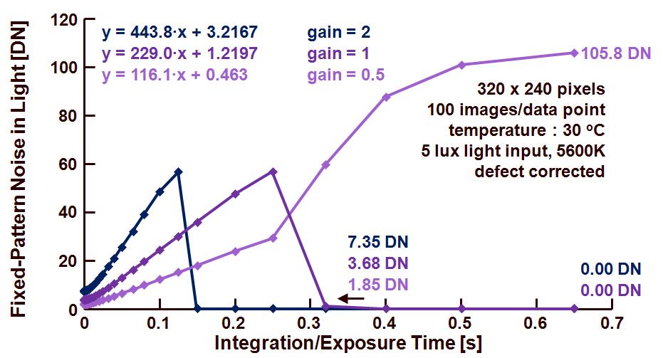
Of interest is the behavior of the FPN as a function of the same exposure time, as shown in Figure 2.  Before calculation of the FPN, the defect pixels were removed from the data set, otherwise the defects will influence the measurement results to a large extend.

120420_blog_2


Figure 2 : FPN as a function of the exposure time.

As was the case in Figure 1, also here the FPN behaves differently depending on whether the ADC or whether the sensor is determining the saturation level.  Two major cases can be distinguished :

       When the ADC determines the saturation level (for gain equal to 2 and 1) : the FPN initially increases in absolute value because of the PRNU, reaches a maximum and then collapses to reach a level of 0 DN.  The latter refers to the fact that the saturation level of the ADC does not introduce any FPN in the case of saturation (apparently this example is using a sensor with a single ADC on-chip),

       When the sensor itself determines the saturation level (for gain equal to 0.5) : the FPN initially increases as well, due to the PRNU, but after a first linear increase, the FPN jumps to a very large value around 105.6 DN.  For exposure times greater than 0.25 s, more and more pixels are saturating and more and more pixels contribute to a large FPN value generated by the anti-blooming transistors.  As can be seen, the final value of the FPN in saturation is 105.6 DN, being equal to 105.6/(2963 – 819) = 4.94 % of the pixel saturation value.

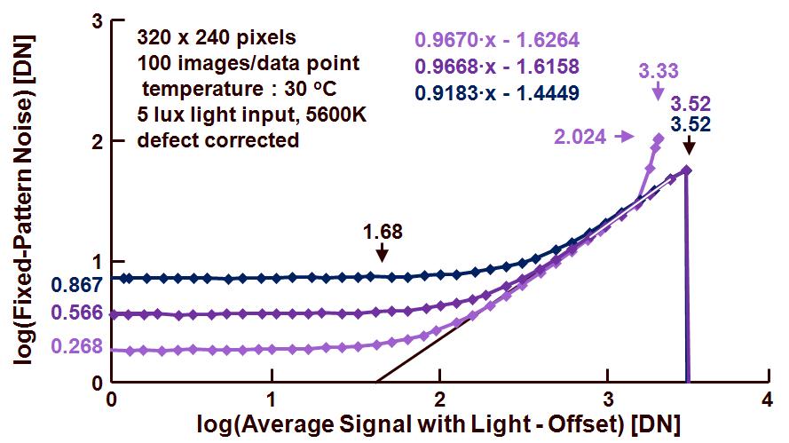
Finally the FPN versus average signal is shown in Figure 3, the figure summarizes both curves already shown in the two previous ones.

120420_blog_3


Figure 3 : FPN versus average signal for various settings of the analog gain.

From this curve the following data can be extracted :

       FPN in dark for the various gain settings is respectively 100.867 = 7.36 DN, 100.566 = 3.68 DN and 100.268 = 1.85 DN,

       The PRNU, independent of the gain setting, is equal to 10-1.68 or 0.0209 = 2.09 %,

       Saturation level is equal to 103.52 = 3311 DN for the gain equal to 2 or 1, and saturation level is equal to 103.33 = 2138 DN for a gain = 0.5,

       In the latter case the FPN at saturation is equal to 102.024 = 105.6 DN or 4.94 % while for the other gain settings, the FPN at saturation is equal to 0 DN.

That concludes the discussion on measuring fixed-pattern noise(s), in dark and with light on the sensor.  Next time the measurement of the temporal noise components will start. 

Albert, 01-05-2012.

How to Measure : Fixed-Pattern Noise in Light or PRNU (3)

April 5th, 2012

Last time the focus in the measurement discussion was on the amount of shading in the average signal under light conditions.  This shading component will contribute to the PRNU, but to fully understand where the sensor’s PRNU is coming from, it might be wise to perform a first PRNU analysis with the shading component included, and a second one after the sensor’s signal is corrected for the shading.  The difference between the two can give a clear insight in the effect of the shading on PRNU.  This will be done in this blog.

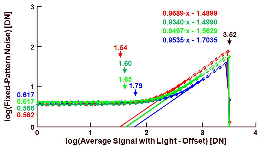
The PRNU data can be also obtained from a PTC-alike curve in which the FPN is plotted versus the average sensor’s signal (corrected for the offset).  This is shown in Figure 1.  Notice that the data on which this figure is based is obtained before any analysis and/or of the shading components.

120328_blog_1


Figure 1 : PTC-alike characterization of the fixed-pattern noise under light conditions, before shading correction.

From the data presented in Figure 1, the following results for the four colour channels (resp. blue, green in blue line, green in red line, red) can be extracted :

       PRNU for the various channels : 10-1.79 = 0.016 = 1.6 % for blue, 10-1.65 = 0.022 = 2.2 % for green in the blue line, 10-1.60 = 0.025 = 2.5 % for green in the red line, 10-1.54 = 0.029 = 2.9 % for red,

       FPN in dark for the various channels : 100.616 DN = 4.14 DN for blue, 100.617 DN = 4.14 DN for green in the blue line, 100.566 DN = 3.68 DN for green in the red line, 100.562 DN = 3.65 DN for red,

       Saturation level of 103.52 DN = 3311 DN.

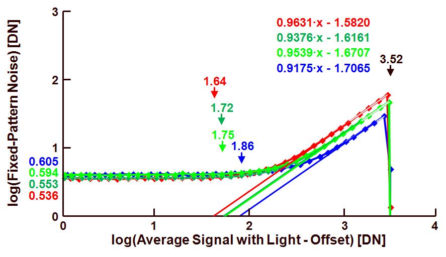
In a next step, the shading can be calculated (as explained in the previous blog) and the aforementioned data can be corrected for the shading.  After correction, the data can be re-analyzed for its PRNU characteristics.  The result is shown in Figure 2.

120328_blog_2


Figure 2 : PTC-alike characterization of the fixed-pattern noise under light conditions, after shading correction.

From the data presented in Figure 2, the following results for the four colour channels (resp. blue, green in blue line, green in red line, red) can be extracted :

       PRNU for the various channels : 10-1.86 = 0.014 = 1.4 % for blue, 10-1.75 = 0.018 = 1.8 % for green in the blue line, 10-1.72 = 0.019 = 1.9 % for green in the red line, 10-1.64 = 0.023 = 2.3 % for red,

       FPN in dark for the various channels : 100.605 DN = 4.03 DN for blue, 100.594 DN = 3.93 DN for green in the blue line, 100.553 DN = 3.57 DN for green in the red line, 100.536 DN = 3.44 DN for red,

       Saturation level of 103.52 DN = 3311 DN.

By comparing the data before and after shading correction is can be learned that correcting the shading is lowering the PRNU numbers (as could be expected).  So one should be cautious with the interpretation of the PRNU numbers : do they include the shading, yes or no ? One may conclude, based on the numbers mentioned here before and after shading correction, that actually the shading does not have that much of an influence on the absolute PRNU numbers.  But the opposite is true !  Even though the PRNU numbers do not reflect a large shading component, it might be present and can lead to unacceptable colour shifts in the images !

See you next time with FPN at saturation.

Albert, 05-04-2012.

Report on Image Sensors Europe 2012 (4)

March 26th, 2012

In this fourth and last report about ISE 2012 I would like to give some more details about 2 presentations.

Firstly the Sony presentation given by Eiichi Funatsu on Small Pixel Technology.  The presenter posted a couple of questions on the screen (when moving from a 1.4 um pixel 8M pixel to a 1.12 um pixel 13M pixel sensor) :

1) Is a 1.12 um pixel giving an acceptable S/N ?  It was shown in the presentation that moving to a flat technology (no STI, no LOCOS) is really improving the dark performance.  Also illustrated was the improvement of the angular response when moving to BSI technology.  So the question could be answered with a YES : the S/N will be acceptable due to new developments and new improvements of the existing technology.

2) Is it really possible to resolve 1.12 um ?  A higher pixel count on the sensor gives the observer a PERCEIVED larger S/N ratio.  For that reason Sony introduces a new parameter, being the Perceived Noise Value.  The method is relying on the resolution characteristics of the human visual system to come up with a quantative indication for Perceived Noise Value.  (More details : Proc. Autumn Meeting of the Society of Photographic Science and Technology of Japan, Dec. 2011, pp. 12-13.)  It was shown that although the 1.12 um pixel showed a worse noise performance, the perceived quality of the image was better than the one obtained by the 1.4 um pixel.

3) Is it possible to use the high resoluting for something else ?  Yes, to extend the dynamic range by the implementation of RGBW colour filters.  This is not new (the presenter mentioned that some other company was doing this already, he did not mention which other company ?!), but what is new is the fact that Sony reconverts the RGBW data in Bayer RGB data.  In this way they still can rely on the existing ISP hard- and software.  Simple, but cleaver idea.

The closing presentation of ISE 2012 was given by Eric Fossum.  It was remarkably that many people remained present at the conference to hear Eric giving his talk.  I have to admit that I had heard this talk already before (it was even posted on YouTube a few months ago), but it is still a pleasure to hear and see the original presentation delivered live by the original author in front of an audience.  Eric has a great style of presenting his material and to bring his ideas about the QIS (Quanta Image Sensor) across.  A few months ago he mentioned that he had a lot of great ideas on the implementation of the QIS, but that he had no money to explore his ideas.  This time he mentioned that he has several PhD students who are going to help him in his research.  So a major step forward !  

Eric Fossum started with a short overview of CCD and CMOS technology, highlighted the short comings of the existing technologies and introduced the QIS which can solve a lot of the problems.  Very wel structured presentation !

Overall the ISE 2012 was a great conference.  Many people gave very positive feedback about the program, the speakers and the content of the presentations.  In this blog only reports are given about the technical presentations and about the contributions on image sensors.  This does not mean that the other presentations that are not highlighted in this blog were of less quality !

Thanks and congratulations to the organizers, and especially to the speakers.  Great job !

Albert, 26-03-2012

Report on Image Sensors Europe 2012 (3)

March 23rd, 2012

This time a bomb of technical data and numbers is thrown out !

First one is coming from the presentation of Hiroshi Shimamoto (NHK).  Their ultra-high definition camera was presented with the sensor having the following specs :

– 7680 x 4320 pixels, 2.8 um x 2.8 um pixel size, 120 fr/s, 12bit resolution ADC, prgressive scan, 8000 ADCs on-chip, conversion tims < 1.92 us, power < 3W, noise < 6 electrons, 96 LVDS outputs in prallel, 0.18 um technology, 1P4M, PPD pixels, 3/2″ optical format, 61.3 dB dynamic range , 0.66 V/lux.s sensitivity, full well < 10,000 electrons. 

The key component of the chip is the column-parallel two-stage pipelined cyclic ADC, being an optimum compromise between speed, power and area.  The ADC was already extentively highlighted during ISSCC2012.  The complete readout of 1 line of information takes up 4 line times : 1) CDS of the column information, 2) conversion of the first 4 bits, 3) conversion of the 8 last bits, 4) reading off chip the digital data.

Here are more numbers, coming from Renato Turchetta’s talk about the work done at Rutherford Appleton Labs.

– X-ray detector based on a stitched mask set (thanks for giving the right reference !) : 14 um x 14 um pixel size, 4k x 4k pixels, 40 fps, 0.35 um CMOS technology, 3T, radiation hardness till 20 Mrad, analog out, on-chip binning and ROI options,

– wafer scale sensors : 2800 x 2400 pixels, 50 um x 50 um, 32 analog outputs, 40 fps, 139.2 mm x 120 mm, 6.7 Mpixel,

– sensors for synchrotron application : 4k x 4k, 25 um x 25 um, 120 fps, HDR with 1: 100,000 at 500 eV, this is still work in progress.

Besides all the data shown by Renato, he also introduced a very nice (and apparently very well received) idea of growing scintillators in cavities etched in silicon.  In a silicon wafer (225 um thickness) holes are being etched (hexagonal in shape and 25 um in size), next in these holes a scintillator is grown.  In this way the conversion and capture efficiency for the visible photons generated by the scintillator is increased.

Also Mark Downing (ESO) had a lot of numbers to report about a CMOS device that will be used in an adaptive optical system to be placed on the biggest telescope of ESO, being 39.5 m in diameter.  The sensor characteristics :

1760 x 1760 pixels, 24 um x 24 um, 0.18 um technology, 6 metal layers, BSI, 4T pixels, 100 uV/e conversion gain, 4k electrons FW, 3.0 e noise, QE > 90 %, image lag < 0.1 %, Peltier cooled to -10 deg.C, power consumption < 5 W,

The chip has in total 70,000 (seventy thousand, this is not a typo) ADCs to comply with the required speed specificiation.  These 70,000 ADC-SS allow to process 40 lines in parallel and offer the option to work at 700 fps.  88 parallel LVDS channels bring the data to the outside.

Albert, 23-03-2012.

Report on Image Sensors Europe 2012 (2)

March 22nd, 2012

Valerie Nguyen (CEA-LETI) opened the show on Wednesday morning.  According to Valerie, the market trend in imaging will be : “Pixels Everywhere”.  If solid-state imaging is going to be used for creating and generating nice images, then the trend will be MORE PIXELS.  But if solid-state imaging is going to be used for control purposes, then the trend will be MORE THAN PIXELS.  Based on existing marketing reports, the year 2009 has delivered 2 M image-sensor wafers with a growth rate of 11 %, and the prediction is that we will get 4 Mwafers in 2015, still with a growth rate of 15 %.  So on the short term, the growth in imaging business is for sure not coming to an end.  But one should realize that in the last 10 years the volume for VGA sensors (as an example) is grown by a factor of 100, but the price went down by a factor of 25 !  A consumer does get more silicon for less money, the manufacturer do get less money for more silicon.

Valerie gave a very nice overview of the imaging activities in the eYe valley around Grenoble.  Apparently a lot of companies in that area are active in solid-state imaging.  She also illustrated what CEA-LETI can do for the imaging industry, such as : thinner BEOL, lightpipes, inner lenses, BSI, colour filter with IR cut-off included, nanoprint for micro-lenses, TSV, etc.  Apparently Grenoble is the place to be for sensor innovations (and maybe also for skiing ?).

Valerie concluded with some statements about the combination of several imaging techniques in one device.  For example micro-bolometers in combination with a visible sensor, or InGaAs underneath Si.  In this way a fusion can be realized between several imaging methods/techniques.  The fusion idea of putting several imaging methods and techniques into one device was mentioned a couple of times by different speakers.

Next was Mats Wernersson (Sony) who convinced the audience that “Mother nature is a bitch”.  He focused on the system aspects of future mobile imaging, and clearly proved that one has to think on system level if one tries to improve the sensor performance.  For instance, low light performance is much more than just sensor sensitivity !  Even if you can count single photons, it is not possible to make nice images with a single photon, but it takes a billion of photons.  Another nice example of the impact on system level of improving the sensor : BSI does allow the use of faster lenses.  So the combination of higher light sensitivity and the possibility of a lower F number is the real benefit of BSI, and this combination is much larger than just the light sensivity increase of the sensor.  Very nice talk with the typical dry humor of Mats.   

Gennadiy Agranov (Aptina) talked about pixel developments.  It is not really new that the industry is going to smaller pixels, but the main challenge is of course to keep up the performance of these tiny small pixels.  Gennadiy showed a lot of interesting data about performance of the devices, for instance QE and dark current of various generations of sensors.  Also worthwhile to mention is the work of Aptina on global shutter CMOS devices.  Over the years they improved the in-pixel storage concept and went from a device with 40 electrons of noise and a QE of 40 % in 2000, to a device with 1.5 electrons of noise and a QE of 85 % three generations later in 2012.  These numbers hold for global shutter devices.  The latter device has a shutter efficiency of 99.96 % (comes close to the transport efficiency of CCDs : 99.99995 %).

In the last part of his presentation, Gennadiy showed the first results about a CMOS device intended for stereo vision.  A single image sensor is used for 3D, based on a pixel with an asymmetric angular response.  Very interesting idea !

Albert, 22-03-2012.

Report on Image Sensors Europe 2012 (1)

March 21st, 2012

Yesterday night, March 20th, the ISE 2012 opened with a keynote of Nobukazu Teranishi of Panasonic.  Nobu is a world-known top-expert in the field of solid-state imaging.  Together with his team at NEC he invented the pinned photodiode and the vertical overflow drain.  But yesteday night he talked about “Dark Current and White Blemishes”.

His talk started with a nice overview of the work Nobu and his team did in the early CCD days to reduce the dark current.  A lot of very basic technology steps were developed at that time to, firstly understand the behaviour of defects in silicon and secondly to optimize the fabrication technology to reduce these defects.  He highlighted all kind of different gettering techniques : internal gettering, external gettering and proximity gettering.  If you listen to the story then it seems all so logical what the various gettering steps can do to reduce the amount of stress in the wafers, to attrack impurities and to reduce the dark current.  But for sure it must have been a work of many manyears to come to the low dark current levels present in today’s devices.

The last part of his talk was about a new dark current generation model for the pinned photodiodes.  Nobu explained that the generation-recombination centers in the p+ top layer and at the interface of the silicon still contribute to the dark current of the PPD.  He supported his theory by means of an analytical model and by applying this model to data published by others.   Ultimately he came to the conclusion that it still is of utmost importance to keep the dark current as low as possible and one way of doing so it to work with devices that have no LOCOS and no STI to isolate transistors, but that all isolation is done by means of implants.  Also this statement seems to be straightforward, but in the CMOS world it appearss to be new, although in the CCD world this technique was already applied a while ago.

Good start of the conference !

Albert, 21-03-2012.

How to Measure : Fixed-Pattern Noise in Light or PRNU (2)

March 13th, 2012

In the previous “How to measure” blog the basic measurement and calculation of the PRNU or Photo-Response Non-Uniformity was discussed. Although the mentioned numbers were not that high, it is always wise to check where the PRNU is coming from. A possible source of non-uniformity with light is shading : a low-frequency component that changes the response of the pixels (e.g. from top to bottom, from left to right, from the middle towards the corners of the sensor). Even if the shading component is small, it can result in (minor) changes in spectral response across the sensor. These type of errors can have a severe effect on colour shading in a colour sensor and can make colour reconstruction pretty complicated. So it absolutely worthwhile to check out the shading under light conditions.

To evaluate the light shading, a similar method can be used as the one applied to evaluate the dark shading. Also the same images are used as before : multiple light images taken at room temperature and at different integration times. To quantify the light shading, the images taken at an exposure time of 80 ms are used : at 80 ms, the average signal is 25 % of the saturation level. Because light shading is the low frequency variation of the signal, the following procedure will be followed :

all images captured at 80 ms integration time are averaged, in this way the temporal noise will be reduced,

the averaged image will be forced through a low-pass filter with a 9×9 filter kernel. This operation will reduce the (high-frequency) FPN.

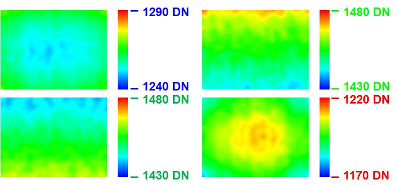
The result after averaging and filtering is shown in figure 1.
120314_blog_1

Figure 1 : low-frequency variation in light signal at 80 ms integration time.

Clearly visible in figure 1 is the non-uniformity of the light signal :

top left is the shading of the blue pixel ; which looks circular symmetric, with its lowest signal value in the center of the sensor,

top right is the shading of the green pixel in the blue line ; which looks to have an increasing signal towards the top of the sensor,

bottom left is the shading of the green pixel in the red line ; which looks to have a decreasing signal towards the top of the sensor,

bottom right is the shading of the red pixel ; which looks circular symmetric, with its highest signal value in the center of the sensor.

The shading illustrated in figure 1 can be expressed as :

the peak to peak value, equal to 20 DN, 36 DN, 30 DN and 41 DN for the four different colour signals,

maximum value, equal to 1270 DN, 1475 DN, 1467 DN, 1211 DN, and minimum value, equal to 1250 DN, 1439 DN, 1437 DN, 1180DN for the four different colour signals.

In principle these numbers are more or less meaningless without any further “reference”. The additional parameters needed are :

evaluation temperature, being room temperature,

integration time, being 80 ms,

dark signal offset, being 819 DN,

average signal with light without offset correction, being 1260 DN, 1457 DN, 1452 DN and 1195 DN for the four colour channels,

average signal with light and with offset correction, being 441 DN, 638 DN, 633 DN and 376 DN.

Taking these numbers into account, the shading in the four colour is equal to 4.5 %, 5.6 %, 4.7 % and 10.9 % of the average sigal measured in each individual colour channel, and measured at 25 % of saturation. These numbers are not really that low, but take into account that not a standard deviation is mentioned, but a peak-to-peak value or a maximum deviation. Do you prefer to have lower numbers : simply reference the shading numbers to the saturation level and they will become about a factor of 4 lower. That is what is called “specmenship”.

Albert, 13-03-2012.
Report ISSCC 2012 (4)

February 28th, 2012

Another nice pair of papers came from NHK and Samsung.  Especially their ADC attracted my attention : both papers made use of what I call myself a tandem-ADC.  This is an ADC that is build around two different architectures or two different working principles.  Last year’s ISSCC had already such a device in a Sony sensor, in which the column ADC was split into two parts : one with counter and one without counter if I remember well.

This time, NHK presented a very similar paper as the one presented at the International Image Sensor Workshop.  It is a 33 Mpixel UHDTV sensor with pixels of 2.8 um x 2.8 um, that is capable of operating at 120 fr/s.  The ADC used was split into two parts, both are cyclic ADCs, delivering in total 12 bits.  The first 4 upper most bits are converted in a first cyclic ADC (based on 3 cycles), the last 8 lower most bits are converted in a second cyclic ADC (based on 8 cycles).  These two cyclic ADCs operate in a pipelined organization, in this way extra speed can be gained.

The second presentation, Samsung’s, discussed a 24 Mpixel APS-C size imager with 3.9 um x 3.9 um pixel size.  The on-chip ADC has a resolution of 14 bits in a full range of 1.7 V.  The circuit realizing the first 2 … 6 bits, in combination with the CDS, is based on a delta-sigma converter.  The remaining 8 bits are converted in a cyclic ADC.  But actually the beauty of this construction is the fact that part of the delta-sigma and the cyclic ADC use the same building blocks.  And because the two parts work in series, several building blocks of the delta-sigma are used as well in cyclic ADC.  In this way the circuitry needed to realize the complete ADC remains relative small.  Cleaver idea !

Talking about ADCs : Delft University of Technology presented a paper on a column-level ADC capable of doing multiple sampling without any increase of hardware.  The ADC is based on an up-counter with BWI (Bit-Wise-Inversion) to allow digital CDS.  In case multiple sampling is applied, the counters simply continue the counting for several consecutive samples.  Without any special pixel design, the multiple sampling (in combination with an extra column amplifier) resulted in a noise level of only 0.7 electrons.  The low conversion gain of the pixel (< 50 uV/e-) clearly indicated further room for improvement.  Pixel noise levels of 0.28 electrons fabricated in “standard” CIS processes are needed for single-electron/photon detection.  This performance level is coming closer !

More to come ? Maybe !

Albert, 28-02-2012.


Report ISSCC 2012 (3)

February 27th, 2012

As I mentioned already earlier, there were a few of “duo” presentations at the ISSCC.  A second pair of papers that pretty nicely went together were two papers on global shutter sensors.

The first one came from Sony, in which a 10 Mpixel device was described.  The novelty of the device was indeed the global shutter, based on a dual storage node in the pixel.  As know the floating diffusion is not really a dark-current-friendly storage node, neither CDS-friendly.  For that reason an extra in-pixel capacitor can be used between the transfer gate and the floating diffusion.  This idea is not new, but in the Sony paper, this extra storage node is relatively small, so it will not occupy that much space.  The extra storage node is only used for very small charge packets and the readout can be operated in the CDS mode.  For larger charge packets, the extra storage node cannot hold all the charges, and part of it will spill over to the floating diffusion.  So in that case a dual storage node is used : the extra in-pixel capacitor together with the floating diffusion.  The latter cannot be operated with CDS, but that is not a real problem, because it plays only a role in the case the charge packet is large (read : and the noise is dominated by photon shot noise).  By itself a simple and cleaver idea, BUT the sensor has a 2×1 shared pixel concept, so every photodiode is provided with an extra in-pixel storage capacitor, but for two photodiodes there is only one floating diffusion.  In other words, the idea presented in the paper can only be applied if the sensor is used in a 5 Mpixel mode instead of the announced 10 Mpixel mode.  To me this was a bit a disappointing conclusion of the paper. 
The device is realized in a 90 nm technology with 1P5M plus a light shield (so is it 1P5M or 1P6M ?).  During the Q&A more info was requested about the FPN and colour, but apparently the device cannot be used in colour mode.

The second global shutter device was presented by Tohoku University.  It was mentioned to be a 1T pixel/s device (not 1 transistor but 1 tera pixel/s !).  The device can deliver 10 Mfs in full resolution and up to 20 Mfs in half resolution mode.  The imaging area has 400 x 256 pixels and every pixel has 128 analog memory cells.  So the device does capture a limited number of 128 frames at high speed.  The memory part is organized above and below the imaging array.  The floorplan of the device looks like a split frame-transfer device (for those of you familiar to CCDs).  The memory cells are made by two capacitors in parallel : poly-poly capacitor and MOS-gate capacitor, with one common poly-layer.  The pixels are 32 um x 32 um, pretty large and have a PPD of almost 16 um in length.  During the author interview I asked the presenter how he solved the issue of image lag within such a large pixel at such a high speed.  Unfortunately I could not get the secrets unrevealed, the presenter promised to me that this will be presented at another conference.  Technology used is 2P4M, 0.18 um, and at full speed the device dissipates 24 W.  Be careful not to burn your fingers !
Amazing movies were shown to illustrate the capability of the high-speed global shutter device.  Very impressive taking into account that the work is part of a PhD project.  Congratulations !

More to come !

Albert, 27-02-2012.

Report ISSCC 2012 (2)

February 23rd, 2012


Yesterday, Feb. 22nd, 2012 the image sensor session took place at the ISSCC.  Several very interesting papers were presented.  For a couple of subjects, there were two different papers presented.  That gives the audience the opportunity to compare two techniques with their pros and cons.  Well done by the organizing committee.

There were two papers, both from Samsung, dealing with the simultaneous capturing depth by means of Time-of-Flight sensors.  But new is the possibility to capture normal video (called RGB) and depth (called Z) information simultaneously.  Simultaneous basically means with the same sensor. 


The first solution captures RGB and Z at the same time.  The device has an image field that was composed out of two types of lines, lines sensitive and optimized for RGB and lines sensitive and optimized for Z.  So for every two lines of RGB there was one line of Z.  The two RGB lines were provided with the classical Bayer pattern, the Z line has no filter at all.  To provide the Z pixel with extra sensitivity, the width of a single Z pixels was equal to the width of 4 RGB pixels.
The pixels not only differ in size, but also in architecture.  The RGB pixels had an extra potential barrier in the silicon and underneath the pixels.  This barrier was not present underneath the Z pixels basically to extend the near-IR sensitivity, because it is the near-IR signal that is used for sensing the depth information.  It was not really clear from the paper whether there was any effort made to protect the RGB pixels from the incoming near-IR light, but in the Q&A the presenter referred to future work to put extra near-IR filters on top of the RGB pixels.

A second solution did not capture the RGB and Z at the same time, but in a sequential way with the same sensor, for instance the odd frames giving RGB and the even frames giving Z information.  The RGB pixels were organized in a 2×4 shared architecture and provided with the standard Bayer pattern.  In the case these pixels were used in the Z mode, a 4×4 binning was done (combination of the charge domain and analog domain) to increase the sensitivity of the Z pixels.  Innovative in this design was the location and sharing of the floating diffusions.  Every single RGB pixel has two floating diffusions (one left and one right of the pinned photodiode) that could be tied together with the floating diffusions of the neighbouring pixels (a kind of back-to-back architecture).  Also at the end of this paper, measurement results and images were shown, both of the RGB and Z results.  During Q&A the presenter mentioned that the RGB images shown were taken with a near-IR filter in front of the sensor and that in the Z-case the filter was removed.

So, two different sensors with different architectures were presented for the same application.  It was clear that in both situations there is still work to do to improve the performance, but nevertheless the two papers gave a clear indication in which direction Samsung (in this case) is seeking after new applications.  

More to come !

Albert, 23-02-2012.