Report ISSCC 2012 (1)

February 21st, 2012


Yesterday, Feb. 21st, ISSCC 2012 started in San Francisco.  In the morning there were the plenary sessions.  They did not had any specific imaging content or imaging information.  In the afternoon during the so-called medical session, a couple of imaging papers were presented.  Here follows a quick report about three of them.

H-S. Kim et al. (KAIST and SAIT) described an X-ray photon counting sensor built-up around a HgI2 photoconductor and a CMOS read out circuit.  The interesting part of the paper was the discrimination in energy level of the incoming X-rays.  In the presented solution, 3 different energy levels could be detected.  The discrimination itself was done in the analog domain by using appropriate thresholding of the peak signal generated by the incoming X-ray photon.  So it is really an X-ray photon counter and based on the peak signal that is detected by the CMOS circuitry, the energy of the X-ray can be classified.

J. Choi et al. (University of Michigan) presented a relative small image sensor that can work in 4 different modes.  In a so-called monitoring mode, the sensor works at 0.8 V in a low power mode.  In the case the sensor (autonomously) detects that it has sufficient energy, it can work at 1.8 V supply and run in a high gain mode (amplification of the signal by a factor 8), a normal mode and a high dynamic range mode (double exposure, both at half the resolution).  The beauty of the design is the fact that the switching between these various mode basically requires a different set-up of the pixel and/or column-level ADC.  This is done by a specific pixel design, such that the pixel circuitry can be used a regular source follower, or they form part of the ADC circuitry.  The basic application for this sensor can be found in wireless sensor networks.

M-T. Chung et al. (Nat. Tsing Hua Univeristy, Hsinchu) presented an ultra-low power sensor, consuming 4.95 uW at a power supply voltage of 0.5 V.  Pixel number 64 x 40 and 11.8 fps.  The sensor converts the incoming information in a pulse-width modulated output signal.  This is realized by an in-pixel comparator based on 5 transistors.  Nice work to see a device operating at 0.5 V.  The author claimed a dynamic range of 82 dB.

The afternoon session started at 1:30pm, and I entered the room around 1:20pm.  At that time all speakers were already sitting on the front rows.  The first view of these front rows scared me a bit : all black haired young guys.  For the old grey man, it was a confrontation with the fact that the new generation is ready to take over, and they mainly come from the Far East.  Nevertheless WELCOME guys, and make sure you have a lot of fun in solid-state imaging !

[If particular papers are not mentioned in my report, that only means that I did not attend the paper  presentation.  Not finding a paper review in my blog does NOT mean that the paper was of low quality !]

Albert, 21-02-2012.


How to Measure : Fixed-Pattern Noise in Light or PRNU (1)

February 14th, 2012


As a logical next step in the “How to Measure” discussion is to look after the non-uniformities with light input on the sensor or Photo-Response Non Uniformity (PRNU).  PRNU is the variation of the output signal from pixel to pixel in the case light is falling on the sensor.  It should be noted that the average sensor signal itself can be composed out of :

       DC offset, introduced by the electronic circuitry, and which is (in a first instance) independent of temperature and exposure time

       Dark current, depending on temperature and on exposure time,

       Photo response, depending on exposure time.

Just like in the case of the average signal, the non-uniformities are calculated (!) based on several images taken in controlled conditions.  To limit the influence of any thermal noise component, several images need to be grabbed, preferably at various exposure or integration times.  Basically, the same data or images as used in the case of measuring the average signal with light input can be reused.  So after averaging all images taken at a particular exposure time to reduce the thermal noise, calculations can take place on the averaged resulting image.  To make sure that the obtained result contains the PRNU and is not too much “contaminated” by the dark current, the amount of light put on the sensor should be large enough to make sure that the photon-generated signal is at least two orders of magnitude larger than the dark-current generated signal.

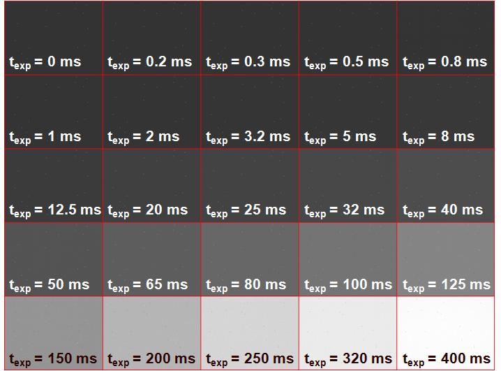
The images used in the calculation of the PRNU are shown in Figure 1 : for 25 different exposure times, the result is visualized in the mosaic image.  Corresponding exposure times are indicated.

next_blog_1


Figure 1 : Sensor output with light input as a function of the exposure time.

The light input conditions are : 5600K colour temperature and 5 lux light input on the sensor surface.  As can be seen from Figure 1, the sensor saturates around 400 ms.  This is due to the limitation of the ADC in combination of the gain setting of the camera.  These effects will be explained and measured later in another blog.  

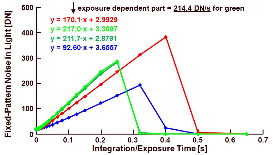
A first way of measuring/calculating the PRNU is to check its behavior as a function of exposure time.  The result of this is shown in figure 2.

next_blog_2


Figure 2 : fixed-pattern noise with light as a function of the exposure time.

There are four curves shown, one for each colour channel.  Please notice that these curves for the PRNU are obtained after correction of the defect pixels !

From the regression line calculated by means of the linear part of the various curves, the following data can be extracted :

       FPN independent of the exposure time, or FPN in dark, being equal to 3.09 DN, (average of the two green channels),

       Time depending part of the FPN, being the PRNU, and equal to 214.4 DN/s, (average of the two green channels).

Taking into account the data obtained (in the previous blog) for the average signal in the various colour channels, the PRNU is equal to :

       Blue channel : 93.6/8770 = 1.06 %,

       Green in the blue line : 211.7/12653 = 1.67 %,

       Green in the red line : 217.0/12715 = 1.72 %,

       Red channel : 170.1/7612.8 = 2.23 %.

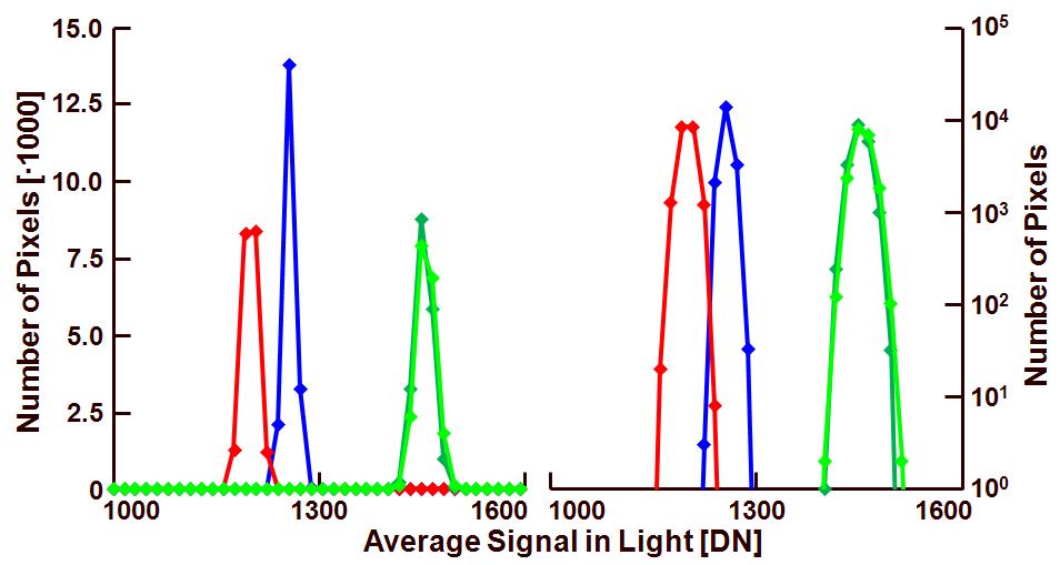
How to express the FPN a sensor or camera ?  In contradiction to the DSNU, the PRNU normally is Gaussian distributed (after correction of the defects and shading, see next blog).  For that reason it is straight forward to express the PRNU as a percentage of the average signal with light input.  This is also done in the above mentioned calculation.  To show the Gaussian distribution of the sensor signal with light input, the histogram of the output (at 25 % of saturation) is illustrated in Figure 3.  The left group of curves illustrates the histogram with a linear vertical axis, the right group of curves shows the same data but with a logarithmic vertical axis.  The latter one is preferred because it shows much better the distribution of deviating pixels (if any) as well.

next_blog_3


Figure 3 : histogram of the average signal in dark.

“There is a warning sign on the road ahead” :

Of crucial importance in this measurement is to measure the PRNU and not the non-uniformity of the light source.  For that reason special attention is needed to create a uniform illumination.  This can be done by :

       Using a point source at a large distance, but in that case the light input will be relatively small,

       Making use of a diffuser in front of the image sensor,

       Imaging a uniform target on the sensor, but in that case the non-uniformity of the lens will be included,

       Using an integrating sphere.  This is most probably the easiest solution, although also integrating spheres do not have a uniformity of 100 %.

In the case of a large imaging array, creating a uniform illumination might be complicated.  In that case a smaller area of the sensor can be used (in the center of the device) and the PRNU can be characterized across this smaller area.  It should be noted that the PRNU values of a smaller area are always more optimistic than the PRNU values of the total sensor area.

Good luck with the PRNU measurements, more to follow next time.

Albert, 14-02-2012.

How To Measure : Average Signal with Light Input

January 28th, 2012


I know it has been a long time since the last technical blog.  As I earlier mentioned, at this time I do have one major problem : TIME !  But I have upgraded my software tools, and here we go again for the first measurement of the sensor with light input.  

Actually, what is the average signal of a sensor or a camera with light input ?  By definition it is the output of the image sensor or the camera when the light sensitive surface of the sensor is exposed to light.  This seems to be very straight forward, but if the measurement data is going to be used to measure for instance the FPN, the uniformity of the light source is very important !  Do not underestimate this item.  

On the other hand, the average light signal delivered by a sensor or a camera will be composed out of :

       A fixed DC offset, very often introduced by the analog circuitry on pixel-, on column- and on chip-level, or by an extra black level offset,

       A photon-generated part, which has a linear dependency on the exposure or integration time as well (at least if saturation of the sensor is not reached, and if a linear pixel is used),

The simplest way to separate the DC offset from the photo-generated part is to perform measurements at several exposure or integration times.   These measurements can be done by means of :

       A good old oscilloscope : in this way one can measure the average output voltage of a sensor or camera.  This method requires a uniform illumination of the sensor.

       The measurement of the reset-drain current, also based on an uniform illumination of the sensor.  This technique is only applicable if the drain(s) of the reset transistor(s) is/are available through a separate connection.  This is the case for CCD imagers, normally this is not the case for CMOS imagers.  So CCDs do offer a very easy way of measuring the average output signal, just by measuring the average reset drain current.  The relation between the measured reset drain current IRD and the average number of electrons in one pixel Npix is given in an earlier blog and will not be repeated here.

       Grabbing images by means of a frame-grabber and a computer.  Once the data of the images is present in the computer, calculation of the average signal becomes very simple.

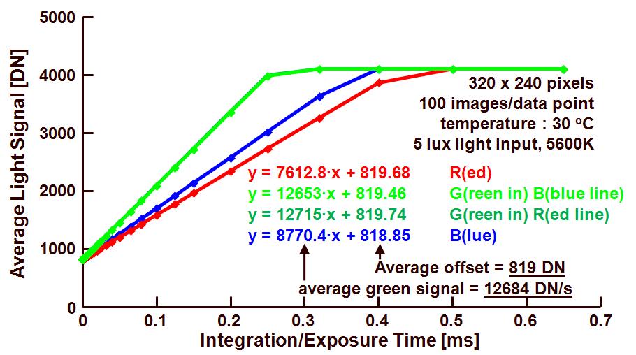
Figure 1 shows the outcome of an average signal measurement with a uniform and constant  light source : at various exposure times and at 30 oC, multiple images are being grabbed, e.g. 25.  At each exposure time all these images were averaged (to reduce the thermal noise) and the averaged image is again averaged over all its pixels (to reduce the fixed-pattern noise).  The amount of light on the sensor is 5 lux, the spectrum has a colour temperature of 5600K and an near-IR filter HOYA500 is included.  In this measurement a sensor with 320 x 240 pixels is evaluated.  So every dot in Figure 1 is the result of 320 x 240 x 25 = 1,920,000 pixels.

120130_blog_1


Figure 1 : average sensor signal as a function of the exposure time, measured at 30 oC.

Figure 1 contains 4 different signals, each representing one of the 4 colour channels : red, green (in the red line), green (in the blue line) and blue.  From the regression lines for the linear parts of the 4 curves, the following numbers can be deduced :

       Offset, independent of the exposure time and in principle also independent of the colour channel, being equal to 819 DN,

       Time depending part of the output signal, representing the photo-generated signal plus the dark current, and equal to 7613 DN/s for the red channel, 12715 DN/s for the green in red lines, 12653 DN/s for the green in the blue line and 8770 DN/s for the blue channel.

 “There is a warning sign on the road ahead” :

       It is clear that the average signal is depending on the exposure time, so accurately measuring or defining this parameter is very important,

       At this moment in the discussion, there is not yet any interest in the temporal noise behaviour of the sensor or camera.  To limit the influence of the temporal noise on the measurements it is recommended to take many images at every exposure time and averaged them on pixel level.  In this way the temporal noise will be averaged out,

       Notice that the measurement is done on the average signal with light input, but at very low light levels, the measurement may be influenced by the dark signal generation.  For that reason it is wise to use quite a bit of light to avoid that the dark signal is “contaminating” the measurement.  A rule of thumb : at every particular exposure time, the signal generated by means of the light on the sensor should be a factor of 100 times larger than the dark signal at that particular exposure time,

       The average signal will change from pixel to pixel (see one of the next blogs) and can also be influenced by a shading component (slowly varying from one side of the sensor to the other side of the sensor).  Non-uniformities and shading are both included in the average output of the sensor on dark.  Or, the average dark signal does not tell anything about the uniformity of it !  To avoid the effect of shading, the sensor signal of a small area (preferably in the center of the sensor) can be evaluated,

       The light sensitivity of the pixels can strongly depend on the angle of incidence.  The sensor response is the largest for perpendicular incoming rays.  For that reason it is advisable to use collimated light input,

       It may sound as a very straightforward requirement, but it is of absolute critical importance that the light source is stable (colour temperature and intensity).  You will not be the first one who is using a AC-powered light source ….

       The measurement presented in this blog is using a colour imager, but it should be clear and straightforward that the same methodology can be used on a monochrome device as well.

Next time the photo-response non-uniformity or PRNU will be discussed.

Albert, 30-01-2012.


Goodbye Max

January 2nd, 2012

Last week, just before the end of 2011, Max Collet passed away at the age of 70.  Max Collet headed the Image Sensor R&D group of Philips Research for about 12 years in the 80’s.  I had the luxury to directly work for him during 16 years, also when he became VP of Philips.  Max was a great phycisist.  He was a genius when it came down to device physics of image sensors.  I, as well as several of my colleagues, learned a lot from him.  Max did not publish that much, neither visited conferences or wrote patent applications, so it will not surprise me that the young generation does not know him, but he was key in the development of the Philips’ CCDs in the 70’s and the 80’s.  When I took over Max position as R&D manager in 1991, he remained my boss till 1999 when the imaging activities were shifted from Philips Research to Philips Semiconductors.  At the time I started working for him in 1983, I asked him what to do.  He answered : “Do whatever you like to do, as long as it is good for the company”. Can anyone think of a better boss ?  I do appreciate Max a lot, not just as a technical person but also as person.  He allowed me to publish my book in 1995, an absolute cornerstone in my personal career.  Thanks Max ! 

Albert.

02-01-2012

Merry Christmas and Happy New Year

December 22nd, 2011

At the end of the 2011 I would like to take the opportunity to wish all my blog readers a Merry Christmas and a Happy New Year.  You are with a lot of people who are visiting my web-site every day.  In 2011, there was a new record established : 785 unique visitors on one single day.  Thanks for stopping by !!!

Looking back to 2011, it was a great year for Harvest Imaging.  The teaching activities continued at full speed, and especially the new course “Hands-on Evaluation of Image Sensors and Cameras” was quite successful.  For 2012, we planned a new location for the course, being Amsterdam.  For me, this will limit the issues with the transport of the equipment.  In 2012, also the very first in-house training of this course will take place.  Of course, all the other courses remain on the calendar and they will be organized at the well-known locations. 

About my consulting activities, I cannot elaborate on these because with several customers I do have NDAs in place that do not allow me to give you details about the projects.  But in summary I can tell that also the consulting assignments kept me more than busy.

2011 was also a great year for conferences and workshops in Imaging.  Personally I could attend the Electronic Imaging in San Francisco, the International Solid-State Circuits Conference, Image Sensors Europe, the International Image Sensor Workshop, Swiss Imaging, and recently the International Electron Devices Meeting.  Unfortunately during the ISSCC I became sick and I had to miss most of the imaging forum on 3D Imaging.  In this way I could optimally enjoy my too-expensive-hotel room because I had to stay in bed for a couple of days.  Highlight of the conferences was the IISW in Hokkaido, Japan.  Despite of the very difficult situation in Japan early 2011, the workshop was very well organized.  Our Japanese colleagues had to set up a plan B to move the workshop from Japan to another Asian country due to the problems after the earthquake and the tsunami.  They did a great job in very difficult circumstances, so that ultimately the workshop could take place as was originally scheduled.  The workshop organization put together a very strong program, based on high-level abstracts submitted by the speakers.  The workshop is and remains the top-event for technical people active in solid-state image capturing.  I heard from several participants attending the workshop for the first time, that they never ever attended a workshop or conference with/in such a great atmosphere as the one in Hokkaido.  Most participants come from competing companies in the imaging market, but at the workshop they are all friends, enjoy technical presentations and discussions, have a chat and a drink together, even sing together in the karaoke bar. 

More or less by coincidence I recently could attend the IEDM in Washington.  My previous visit to IEDM in Washington was 6 years ago.  At that time I presented my work on the cosmic ray damage.  One of the reasons to attend this year’s IEDM was my nomination for the IEEE Education Award. 

2011 was a bit of a sad year for my activities at the Delft University of Technology.  Unfortunately one of my former co-workers passed away at a way-too-young-age.  I mentioned this in one of the previous blogs that Hiroaki Fujita, who worked for me during one year in Delft, died recently.  On the other hand, 3 out of my 5 PhD students finished their projects.  So at this moment, the population of my group in Delft is a bit thin.  Initiatives to raise funds for new programs have been taken, but it is not that easy anymore to get money for PhD projects.

What is happening to me more and more : I do meet much more people than ever before that seem to know me, but that I apparently do not know of.  I do see/meet more and more people through my courses and at conferences, but unfortunately I cannot store all the faces, names and affiliations on my “hard disk”.  So please forgive me if I meet some of you and if I do not immediately recognize your face.  I guess that I saw about 3000 people in my courses over the last 10 years, so it is impossible to know them all.  Sorry for that.

I wish all of you the very best for 2012, and hope that we will regularly “meet” through this blog.  Thanks for visiting the website of Harvest Imaging, hopefully see you next year 😉

Albert, 22-12-2010.


How To Measure FPN in Dark : Wrap-up

December 15th, 2011


Several blogs are spent on the measurement of fixed-pattern noise in dark.  How far are we now, which parameters are on the table ?  As a kind of wrap-up, the following was measured and reported for the dark current (obtained at room temperature) :

       Offset of the signal in dark : 819 DN,

       Average dark signal : 0.1025 DN/ms,

       Dark signal at 25 % of saturation or at 8 s integration time : 1637 DN, after offset correction : 818 DN,

       Number of ADC-bits : 12,

       Head room for the video signal : (212 -1) DN – 819 DN = 3276 DN.

And for the FPN in dark the following values were found (all numbers obtained at room temperature and after correction of defect pixels) :

       Total FPN :

o   FPN part independent of the exposure time, being equal to 3.9 DN,

o   time depending part of the FPN, being the dark current FPN or DSNU, and equal to 0.0186 DN/ms.  At an average signal level of 25 % of saturation and/or an exposure time of 8 s, the DSNU can be expressed as :

§  maximum value of dark signal : 2905 DN, or after offset correction : 2086 DN, and,

§  minimum of the dark signal = 1373 DN, or after offset correction : 554 DN,

§  peak-to-peak value of 1532 DN,

§  root mean square (rms) value equal to 150.5 DN,

§  the rms value of the DSNU can also be expressed as 18.4 % of the average signal at 25 % of saturation,

§  or is equal to 4.6 % of the saturation level of the sensor,

§  the DSNU has a median value of 1600 DN, after correction of the offset equal to 781 DN,

       Column FPN :

o   2.9 DN is the FPN at 0 s exposure time,

o   the time depending part of the column FPN equals to 0.0008 DN/ms.  At an exposure time of 8 s or at 25 % of saturation level, the column FPN :

§  equals to 7.8 DN rms or,

§  taking into account the absolute values mentioned earlier, the column FPN can be calculated to be equal to 0.95 % at 25 % of saturation, or 0.24 % of the saturation level of the sensor.

       Row FPN :

o   2.4 DN is the FPN at 0 s exposure time,

o   the time depending part of the row FPN equals to 0.0116 DN/ms.  At an exposure time of 8 s or at 25 % of saturation level, the row FPN :

§  equals to 92.8 DN rms or,

§  taking into account the absolute values mentioned earlier, the column FPN can be calculated to be equal to 11.4 % at 25 % of saturation, or 2.84 % of the saturation level of the sensor.

       Dark shading or low-frequency dark signal variation :

o   the peak to peak value equals to 561 DN,

o   a maximum value of 2116 DN, or 1297 DN after correction of the offset, and,

o   a minimum value of 1555 DN, or 736 DN after correction of the offset.

Taking the FPN numbers at 0 s integration time into account, one can state that 2.9 DN is coming from the column FPN, 2.4 DN is coming from the row FPN.  To complete a total FPN of 3.9 DN, the pixels themselves contribute 1.0 DN.  In other words, the FPN measured on pixel level is mainly coming from the column and row circuitry.

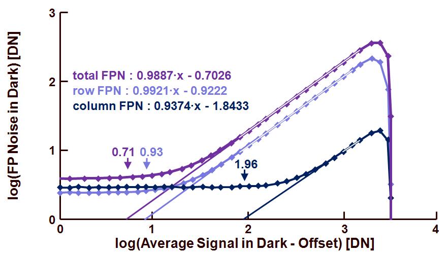
To conclude this chapter about FPN in dark, the obtained results are summarized in figure 1,  showing the fixed-pattern noise as a function of the average effective dark signal (= corrected for the offset).

111215_blog_1


Figure 1 : Overview of the results obtained from the fixed-pattern noise measurements.

Shown are the total FPN, the column FPN and the row FPN.  At the crossing of every curve with the vertical axis, the FPN at an integration time equal to 0 s can be found :

       total FPN : 100.593 DN = 3.92 DN,

       column FPN : 100.464 DN = 2.91 DN,

       row FPN : 100.385 DN = 2.42 DN.

At the crossing of the extrapolated curve (with slope = 1), and the horizontal axis, the DSNU can be found :

       total DSNU : 10-0.71 = 0.195 = 19.5 % (18.4 %),

       column DSNU : 10-1.96 = 0.011 = 1.1 % (0.95 %),

       row DSNU : 10-0.93 = 0.117 = 12 % (11.7 %).

The numbers between brackets are the ones obtained through straight-forward calculation shown at the top of this blog.  They illustrate the accuracy of the curves shown in figure 1.

In principle there is one FPN of interest still missing, being the FPN at saturation.  This will be discussed at the moment the non-uniformity with light will be studied.

PS Some numbers mentioned in this blog deviate from previous blogs, due to corrections.  Sorry about that.

Albert, 15-12-2011.

Goodbye Hiro.

December 11th, 2011
 
In 2002 I was contacted by a young Japanese engineer with the request to spend a 1 year sabbatical at the Delft University of Technology.  It turned out that the young engineer was working for Sony, and that Sony fully supported the initiative of staying 1 year abroad.  At that time I had a very small group of researchers working on CMOS image sensors at the University, and extra manpower was more than welcome.  So within a couple of days an agreement was set up between the University and Sony, and only a few weeks later the engineer arrived in Delft.
 
When the University’s security called me up and told me that a visitor arrived for me, I went to the elevator to wait for the Japanese engineer.  When he stepped out of the elevator, a tall, skinny, happy-faced person stepped to me, and introduced himself.  Then he asked : “How shall I call you ?”.  That particular question immediately illustrated to me that this was the right person, taking innitiative, not shy even not in a foreign culture.  He said : “You can call me Hiro !”.
 
Hiro worked for me during 1 year.  He focused on the simulation of noise sources in a CMOS image pixel.  We had a great time together.  He was enthusiastic, always open-minded, and with a very great sense of humor.  He talked about his family, about his friends, about the Japanese culture, about traditions, and other subjects, he never talked about his employer Sony.  That was also something I very much appreciated.  He kept the industrial secrets for himself, the way it should be.
 
After his sabbatical year, Hiro did not join Sony again, but he went for an American adventure.  He decided to work for Kodak in Rochester.  To me this was a bit a strange choice, because I think that Sony invested in him to widen his technical expertise and not to widen his horizon with a contract to Sony’s competitor.  Anyhow, it was Hiro’s choice and Sony as well as myself respected that.  The contacts with Hiro became loose, till I met him a couple of years ago at the IEDM in San Francisco.  We had a nice dinner together in a Japanese restaurant.  The conversation we had was again very open, lively, with a lot of jokes, humor and fun.  He told me that he was going to marry, he seemed a very happy man to me.  Later on he sent me a mail with the message that he became a father.
 
Unfortunately, very recently the message arrived on my PC that Hiro passed away, while he was back in Japan.  I have no idea what happened to him, it turned out that he was hospitalized, but that is all I know about it.  When the sad message reached me, I was absolutely shocked.  Such a young, lively, intelligent person was no longer with us.  I think that most of the people active in the imaging community will not know Hiro, but the few that do know him, will all agree : we lost a great personality, a great friend, a great colleague.  I would like to wish his family all the strenghts that they need to overcome their great lost.  I do have the great memory of Hiro and I am very happy that I could get to work with him.  To paraphrase someone “Hiro, we would have liked to know you better and will miss your not being here”.  Goodbye Hiro !
 
Albert.
11-12-2011

Report : CMOS Detector Workshop, Toulouse, Dec. 7th, 2011

December 8th, 2011

Digital Focal Plane arrays for Cooled Infrared Detectors – SOFRADIR

          It was emphasised that column level ADCs are best to achieve good resolution and power consumption.

          The 1st generation designed imager in 0.35um technology had a pixel pitch of 15um, 640×512 pixel array, SNR of 77.3dB and a power consumption of 70mW at 80Hz.

          The ADC pitch is 50um, 15-bit resolution and consumes 70uW/ADC.

          2nd generation imager was claimed to perform better but no specifications were provided.

IR Sensor for space applications at Selex Galileo – Selex Galileo

          Design of Mercury Cadmium Telluride (MCT) avalanche photodiode was presented.

          The desired specifications are a noise floor of less than 1.5e-, operating temperature of greater than 200K, QE greater than 70% and a bandwidth of greater than 20MHz.

          The devices showed no major change in dark current after radiation.

          The devices are sensitive to 2.051um wavelength but are also suitable to work between 1.3-2.2um.

          MCT-APD wavefront sensor was designed. It was mention that the avalanche gain does not affect non-uniformity and depends only on voltage biasing and alloy composition. A 1.75e-/pixel readout noise with an APD gain of 33 was reported. The noise increased to 2.8e- when operated at 5MHz speed with the APD gain of 33.

Innovative ROIC for very low flux sensors – SOFRADIR

          The gate capacitance of source follower helps in noise reduction and a 4fF capacitor based readout has been developed and reported. The innovative designs were claimed but not shown!

          For a 18um pixel pitch a total conversion capacitor of 27.3fF and for a 15um pixel pitch a conversion capacitor of 20fF was reported. It was claimed that these conversion capacitors are the state-of-the-art. The author referred to their paper to be published in Journal of Electronic Material, June 2012 for more details.

          Other performance parameter mentioned were a conversion gain of 5uV/e-, dark current of 0.06e-/s, read noise of less than 6e-, leakage current of 0.002e-/s, power consumption of 360uW/100KHz, operating temperature of 70K and operated in rolling shutter mode.

          PTC was not used to derive the conversion capacitors rather CNES developed in house capacitance measurement tools that were used. It was pointed out by the audience that the inter-pixel capacitance will affect the total capacitor measured which was not taken into consideration.

Specifications of an Analog-to-Digital Converter for uncooled infrared readout circuits – ULIS

          NETD (noise equivalent temperature difference) which is equivalent to SNR is used to characterize the sensor behaviour.

          Non-linearity versus temperature behaviour was shown to be around 1%. Different gain and offset correction were applied for each pixel.

          The desired ADC specifications mentioned were a resolution of 14bits, ENOB of 12.5bits, Sampling frequency greater than 7MHz for QVGA and greater than 20MHz for VGA configuration, INL less than 2LSB and the power consumption of less than 80mW for QVGA and less than 100mW for VGA with a supply voltage of 1.8V.

          The measured ENOB was 12.8, SNR of 79dB, DNL of 0.76, INL of 4.93, THD of -72dB and a power consumption of 95mW at an operating speed of 5MHz and a supply voltage of 5V was presented.


CTIA circuit for low light level imaging with InGaAs detector. Demonstration with a 15um pitch VGA format.

          Advantages of InGaAs SWIR detectors were presented.

          A CMOS imager with a CTIA pixel was described. The tricks to optimize the noise performance of the CTIA amplifiers were mentioned. Limiting the bandwidth by adding an output load helps in noise reduction.

          The image sensor was designed in 0.18um technology and had a resolution of 640×512, pixel pitch of 15um, can be operated at 120fps or 60fps in rolling shutter mode, dual gain for day/night operations and the reported noise without CDS was 130e- (Integration time of 8ms, Temp. Of 30C) while with CDS it was 90e-. The dark current was reported to be less than 20nA/cm2 and was claimed to be the state-of-the-art (the integration time used was only 8.3ms). The input referred noise with CDS was mentioned to be in between 30-40e- depending on photodiode bias voltage.

          The dual gain mode was used. In high gain mode a conversion gain of 17.6uV/e-, full well of 105Ke-, read noise of 30e- with CDS and a DR of 71dB was reported. While in low gain mode the conversion gain achieve was 1.9uV/e-, full well of 1Me-, read noise of 80e- with CDS and a DR of 82dB was reported.

Optimization of perfomence of Backthinned CMOS devices – e2v

          To improve the red QE, thick epitaxial layer is needed.

          MTF was defined as the ratio of undepleted thickness to the pixel pitch.

          Standard 12um thick epi was thinned to 7um, which 18um thick epi was thinned to 11um.

          A responsivity of 39uV/e-, noise of 5-20e-, peak signal of 49ke-, QE of greater than 80% for spectral range of 450-750nm, dark current of nearly 60e-/pixel/sec at 313K was reported for a pixel pitch of 7um operating at 7.7MHz. A PRNU was mentioned to be good on the back thinned sensor especially for shorter wavelengths.

          It was mentioned that the shape of the photodiode shows differences in the horizontal and vertical MTF, not significant though.

          Further it was mentioned that if microlenses are used together with frontside pixel then back thinned provides limited advantages in terms of QE. Further thinning too much would pose wire bonding problems as the metal would become too thin and would be prone to be displaced or damaged.

          In the discussion it was also mentioned that smaller PPDs have small depletion region and thus shows poor MTF.

Results of the second generation hybrid backside illuminated imagers and an introduction to other high-end imager development at imec. –imec

          The first generation hyper spectral imagers had a QE of greater than 80% in the spectral range of 400-800nm, however they suffered from high cross talks.

          In the second generation hybrid imagers, an optimized 2 step graded EPI for built-in electric field was used. CuSn bump technology was used instead of Indium bonds. The functional bonds were reported to have a yield of 99.99%. The trenching was improved too. This all resulted in good QE and cross talk values. Further it was mentioned that these devices were radiation hard designs.

          The imager was designed in 0.13um imec CMOS process. The pixel pitch as 2.5um, resolution of 8Mpixel, 12 bit sigma-delta ADC operating at 60fps, imager size of 14x13mm taped out and expected to be characterized early next year.

CMOS image sensor pixel with 0.5 noise electrons RMS – CAELESTE

          The RTS noise and 1/f noise is reduced by cycling the MOSFET between inversion and accumulation to produced un-correlated noise which when sampled become “white”.

          A CTIA configuration was used and a very high conversion gain of nearly 1000uV/e- was reported.

          When the cycling of the MOSFET was not used a 2e- readout noise was obtained. While when the cycling was performed a 0.5e- readout noise at dark was measured. However it mentioned that the measurements showed variance and it might be due to the CVF. The research institutes and PhDs were invited to do an independent confirmation!

Radiation effects on CMOS image sensor – ISAE

          Discrimination of TID induced DC-RTS and DDD (displacement damage dose) induced DC-RST was done.

          Meta-stable generation centers in PPD causes signal variations.

          DC-RTS increases proportionally to TID.

          It was mentioned that bulk defects located in the space charge region responsible for DDD induced DC-RTS while interface states located in the trench oxide are mainly responsible for TID induced DC-RTS.

          The Co60 used for radiation measurements would also produce point defects which can generate undesired RTS. This was mentioned in the discussion.

A round table discussion was also held on “Is there a place for a common strategy for the end users” and it was pointed out by an ESA representative that CMOS cannot compete with CCD in low volume space applications as long as the foundries and companies working on CMOS don’t discuss or reveal more information. Information sharing would be keen to see the CMOS image sensors being actively pursued in low volume applications.

Written by M. Sarkar.  Thanks to Mukul for the effort of putting the 2 reports together on such a short notice and for sharing the reports with the imaging community.

Albert.

8-12-2011.
Report : CMOS Detector Workshop, Toulouse, Dec. 6th, 2011

December 7th, 2011

Characterization Results of Teledyne DALSA High Bandwidth Matrix and Linear CMOS Device and Roadmap for Radiation Hard and High Resolution Area Devices – DALSA

          IT-K2 family of image sensors for colour imaging and X-ray products was described. The dual line 7um pixel have full well capacity if 30ke- while the single line pixels have a pitch of 3.5um.

          The FPN reported was less than 40DN, conversion gain of 0.126DN/e/line, noise floor of 12e-and dynamic range of 66dB, PRNU less than 10% and non-linearity of less than 2% between 10-90% saturation signal was reported.

          Over exposure detection circuit before CDS block was used to remove the overexposure artefacts.

High QE, Thinned Backside Illuminated 3e- RoN, Fast 700fps, 1760×1760 Pixels Wave Front Sensor Imager with highly parallel readout – ESO

          Imagers to image the natural guide star and laser guide star was described.

          A 4T rolling shutter (in chunks of 20 rows) with a pixel pitch of 24um, responsivity of >100uV/e-, Full well of 4ke-, Read noise of less than 3e- rms, QE of greater than 90% in the visible region and a lag of less than 0.1% was reported.

          The desired dimension of the imager is 50 x 60mm2. One serious problem with huge imagers would be to drive the clocks over such huge length. The presenter presented an idea of using primary and secondary clocks and synchronously switching ON/OFF the stitched channels to solve the clocking problem over long distance.

L2CMOS Image Sensor for Low light Vision – e2v

          Light from night sky provides photons mostly in the NIR region of the spectrum thus QE improvement in this region would be very beneficial.

          QE improvement by deep depletion is proposed.

          Pixel pitch of 5.3um, Full well of 50ke- and total noise of 3.1e- rms (ADC noise of 1.5e-, Pixel SF noise 2.2e-) at 25 frames per second was reported. A surface channel source follower was used.

          Some pictures were shown at 0.0011 lux (starlight) at 20fps. Interesting pictures and video shown. Very noisy but interesting.

          Because of the deep depletion, diffuse electrons are also collected thus images formed are less focussed, a side effect clearly seen in the pictures shown.

Fast Response, Low Noise, Multiple Shutter, Non-destructive readout Line Sensor for Spectroscopy Applications based on lateral drift field photodiode principle – Fraunhofer

           The LDFD (lateral drift field photodiode) principle was used in optical excitation spectroscopy. The photomultipliers has been used in those applications primarily due to its high response time (nearly 100ns).

          The principle of LDFD is a concept similar to CCD and p+ pinning. The n-well doping concentration is increased in the direction of the sense node.

          10um pixel pitch was shown, it was mentioned that work on 5um pitch is in progress.

          A dark current of 41pA/cm2 and a response time of 3.5us are shown. The fill factor is claimed to be 100% which is not true as a channel stop of 2um is used (good catch from the audience).

ESA supported development in CMOS imaging sensors – ESA-ESTEC

          An overview of image sensor programs with ESA was presented.

          Back side illuminated thinned hybrid image sensors were developed together with imec. The sensors specifications were read noise of 25e-, full well of 0.4Me-, QE of greater than 80% over 270-400nm, pixel pitch of 20um with an array size of 1024×1024 was reported.

          Back side illuminated thinned monolithic image sensors were developed together with CMOSIS. The reported figures for the desired imager were pixel pitch of 15-25um, full well of 0.5Me-, QE of greater than 70% over 350-800nm and a read noise of 50e- rms. The kick off will be in Jan. 2012.


CMOS Image sensor for lunar mission – CMOS Sensor Inc

          Two imagers for lunar mission, a line sensor with 4000 line elements and an array sensor with a 256×512 array was presented.

          The line sensor had a pitch of 7um, 12 bit resolution, DR of 123.2dB (the DR was calculated using the output of destructive load over non-destructive load, if the noise is used then the sensor would have a DR of 50dB with a noise of 68DN) and non-linearity of less than 0.1%.

          The array sensor used a pixel pitch if 50um, 12 bit ADC and had a non-linearity of less than 0.5%.

          Beautiful pictures of moon and earth were shown. 

          The FPN and dark count for linear sensor was shown to increase after TID of 100krad.

High Speed BSI CMOS Image Sensor for space applications with 1.1Me- full well capacity and 28e- rms read noise – BAE Systems Imaging solutions

           A hyper spectral imaging within the project EnMap was presented.

          A pixel pitch of 24um, 5T pinned photodiode, full well of 1.1Me-, spectral range of 420nm-980nm, DR of greater than 1500:1, read noise less than 70e- for high gain and less than 200e- for low gain TID of 14.51 with a power less than 2W is desired.

          The QE was shown to be 85% at 600nm, a conversion gain of 1uV/e-, a dark current of 150e-/pixel/ms at 293K and a read noise of 27e- when operated in rolling shutter mode while 44e- when operated in global shutter and a 50% MTF at Nyquist was shown to be obtained.

          The single event upset for particle beams of 1.6MeV and 42.5eV was shown to cause an increase in the readout noise by nearly 10% while the conversion gain and the dark signal were not affected much. The non-linearity for high gain increased marginally while for low gain it was minimum.

          Image lag is important for 24um pixel pitch, and it was raised in the question and answer session. The image lag is kept low by segmenting the pixel into a mosaic kind of structure. This keeps the overall image lag low.

Characterization of a digital TDI CMOS demonstrator for high resolution earth observation –CMOSIS

          A TDI demonstrator for high resolution earth observation applications was presented.

          50TDI stages with a pixel pitch of 13um and 1500 columns (to be increased to 6000 columns) with a 10 bit cyclic ADC as shown. The readout time was around 1.3us, with a 70uV/e- conversion gain, 3e- read noise, full well of 130ke-, good linearity, no image lag and no “black sun” effect observed while a QE if 55% at 550nm was reported.

          It was reported that column ADC reaching a speed of 1.4MPS caused stability problems, may be due to the reference voltage instability.

Written by M. Sarkar

7-12-2011

Report : Solid-State Image Sensors at IEDM, Dec. 5th, 2011

December 6th, 2011


Paper 1 : Extremely-low noise CMOS image sensor with high saturation capacity, by K. Itonaga (Sony).

It was reported that for S/N in dark it is primarily needed to lower the noise floor of the sensor.  This can be done by optimizing the technology to lower the amount of defects and/or by increasing the area of the source-follower transistor.  On the other hand, to increase the S/N at bright conditions, it is needed to increase the saturation level, for instance by choosing a larger PD area.  In this paper both items are improved and optimized.  The level of defects is reduced by no longer making use of STI in the image part.  The complete pixel array is made on the same gate dielectric and isolations are introduced by means of p+ implants.  As a result the 1/f noise is going down as well as the dark current.  The technology was demonstrated by means of a 16 Mpixel sensor, 1.12 um pixel, 15fps.  The pixels are configured in as 2 x 4 shared pixels, without a select transistor resulting in 10 transistor per cell of 8 pixels (1.25 T/pixel).  Noticable, the length of the source follower gate is 1.14 um, being the optimum between thermal noise and 1/f noise.  Nice paper, but unfortunately no performance numbers were given during the presentation.

Paper 2 : High performance 300 mm backside illumination technology for continuous pixel shrinkage, by D. Yaung (TSMC).

The author reported about several issues encountered in the development of the BSI process, and told us that they were solved by further optimization of the tools, by reducing particles, by reducing defects, etc.  Results were shown to illustrate that the BSI process is under control, for instance the 1/f noise of the source-follower in the BSI process is better than the 1/f noise of the source-follower in the FSI process.  QE values for a 0.9 um pixel were shown : 50 % in blue, 47 % in green en 45 % in red.  The pixels were realized in a 65 nm process with a remaining thickness of the silicon equal to 2 um … 4 um.  In the case of the 0.9 um pixel, the optical cross-talk is about 4 times as large as in the 1.1 um version.  As can be expected, the QE and the optical cross-talk, both become worse if the pixels shrink.  Simulated data for pixels down to 0.6 um were shown. 

Paper 3 : A 1.4 um front-side illuminate image sensor with novel light-guiding structure consisting of stacked lightpipes, by H. Watanabe (Panasonic).

The major FSI limitations are the reduced aperture size of the pixels (coming close to the wavelength of red light) and the propagation distance (several um).  The newly developed technology is characterized by :

          45 nm Cu metallization technique, this allows a very low optical stack,

          Stacked lightpipe consisting of a high-refractive index material (Si3N4) and separation wall (SiO2) between the colour filters.  So in principle, the colour filters already act as a lightpipe.

Some data : QE in green 74 % in comparison with 69 % for the BSI and 43 % for the FSI without stacked lightpipe.  Angular response is 80 % at an angle of 20o.  Further demonstration is done by a 14 Mpixel device with 1.4 um pixel size and a dark current of 9.9 e/s @ 60 oC.

Nice paper with good results and a good presentation.

Paper 4 : Investigation of dark current random telegraph signal in pinned photodiode CMOS image sensors, by V. Goiffon (ISAE).

CMOS image sensors demonstrate blinking pixels due to current fluctuations in the source-follower (SF-RTS) and dark current fluctuations in the photodiode (DC-RTS).  The paper concentrated on the latter effect.  The frequency of the DC-RTS blinking pixels seems to be much lower than the frequency of the source-follower RTS pixels.  The authors built their own analysis tool based on edge detection in the temporal domain.

The following experimental observations were made :

          DC-RTS depends proportionally on the integration time,

          There seems to be no correlation between the RTS pixels and the dark current in the bright pixels,

          There seems to be no correlation between the RTS pixels and the average dark current,

          There seems to be no correlation between the switching time of the RTS pixels and their amplitude,

          Activation energy seems to be 0.6 eV.

          When the TG is put into accumulation, all RTS pixels are gone !

In conclusion : the DC-RTS pixels are metastable defects characterized as a SRH generation center, that are located at the STI edge or at the depletion edge of the transfer transistor !

Very well structured paper, with a lot of experimental data.


Paper 5 : A CMOS compatible Ge-on-Si APD operation in proportional and Geiger modes at infrared wavelengths, by. A. Sammak ((TU Delft).

The author described their technology flow to make ultra-shallow p+ junctions.  This is based on the deposition of pure B on Si or pure Ga on Si.  For the Ge-on-Si devices, they propose to use the combination of pure Ga on top of pure B on top of Ge.  Devices were made and first results were shown also for the near-IR spectrum.


Paper 6 : Enhanced angle sensitive pixels for light field imaging, by S. Sivaramakrishnan (Cornell Universy).

Angle sensitive pixels based on dedicated metal grids were already demonstrated at previous conferences.  One of the drawbacks of these devices is the presence of the double metal grid.  This reduces the quantum efficiency to 12 %.  In this paper two new techniques were introduced to overcome the issues of quantum efficiency :

          The bottom metal grid was replaced by means of 2 interleaved finger-structured diodes,

          The top metal grid was replaced by a phase-grating in SiO2.  The latter is processed later in-house with simple processing steps, but the width of the phase-grating is defined by a metal grid defined by the CMOS processing fab.  After the phase-grating is defined, the metal mask is removed.  Very cleaver solution to obtain very fine linewidths defined by the fine-detail CMOS process, but ultimately generated by classical etching tools.

At the end of the road, an angle sensitive device is realized without any metal grid above the pixels.  The QE obtained was reported to be around 45 %.


Paper 7 : A 192×108 pixel ToF-3D image sensor with single-tap concentric-gate demodulation pixels in 0.13 um technology, by T.-Y. Lee (Samsung).

A device is developed with 192×108 pixels, 12 bit ADC built in a 0.13 um.  The light source for the ToF measurement is an LED with 850 nm wavelength.   The pixel pitch is 28 um, and is using a single tap solution for the detection of the incoming signal.  Although this single tap gives pretty good results, it should be noticed that 75 % of the incoming information is not used.  The measurement error is smaller than 1 % for distances up to 7 m.

The detection contrast and the quantum efficiency are essential parameters in ToF sensors.  The QE can be further optimized by going to BSI.  Other options for further improvements are the optimization of the light source,  optimization of the optics and implementing a correction of the ambient light.

Albert

05-12-2011.