“Imaging Sensors” course at Delft University of Technology

January 15th, 2013

Together with my colleague Edoardo Charbon, we developed a new course on Imaging Sensors.  The course is intended for students of the first year of our international EE MSc program.  We had 28 students which chose to follow the class.  Quite a nice success.

Why do I put this message in my blog ?  Well to tell you about our examination procedure.  Instead of asking the students to learn all kind of definitions by heart, we gave them a list of about 50 technical publications, material that came mainly from IEEE and IISW.  We asked to all students to select one publication, study it, make a poster of it and then explain the material by means of the poster to the two professors and their colleague students.

We just had the poster sessions last week, and overall the students did very well.  It is amazing to see how easily these young people pick up the ideas presented in the publications and how they explained it to the audience.  A big advantage of this way of examination is the fact that you learn something from it yourself.  It is really funny to see your own ideas explained by others in a way that is completely different from the way I would have done it myself.

So in conclusion I think it was a very successful experiment, worthwhile to repeat in the coming years.

Albert, 15-01-2013.

Merry Christmas and Happy New Year

December 17th, 2012

Time flies, almost at the speed of the old Concorde airplane, 2012 is almost over ….  So like every year I would like to take the opportunity to wish all my blog readers a Merry Christmas and a Happy New Year.  You are with a lot of people who are visiting my web-site every day.  In February 2012, there was a new record established : 856 unique visitors on one single day.  This is really incredible, especially the short conference reports that I am posting attract a lot of readers.  Thanks for stopping by !!!

Looking back to 2012, it was again a great year for Harvest Imaging.  The training activities continued to be successful.  Although a few scheduled courses had to be cancelled, about 90 % of the scheduled events could take place.  I am very happy with this high hit rate, taking into account the number of courses I am running every year and taking into account the economical issues our industry is facing.

In 2012 I had the opportunity to attend again a couple of interesting conferences and to meet a lot of enthousiastic imaging fanatics.  Unfortunately I had to abstain from the Electronic Imaging conference because of obligations with a PhD defense.  This was really a bad coincidence, because I was honoured with the Award of Electronic Imaging Scientist of the Year.  After all not a bad coincidence for my daughter who went to San Francisco to replace me and to pick up the award.  Remarkably successful was the Image Sensor Europe conference held in London (UK).  A great set of speakers, attractive topics and a nice new location.  I am curious to see whether the ISE2013 organizers can keep up the same quality level as in 2012, hopefully they will.

Two smaller Fraunhofer workshops in Germany were attended : the CMOS workshop in Duisburg and the Microoptics Imaging and Projection in Jena.  The Duisburg one was organized already for the 6th or 7th time, for the Jena one, it was the 1st time.  I for sure enjoyed attending the latter, a bit off topic for me, but a lot of new things to learn.

Finally at the end of 2012 my new office became available.  During the Christmas holidays I will move my stuff out of my own house into the brand new office space.  I do hope that the new location will stimulate the creativity as much as my office space in our living room did.

To conclude, I wish all of you the very best for 2013, and hope that we will regularly “meet” through this blog.  2013 is announcing itself as going to be a very interesting year, because he is coming to Europe !!!  The Summer of 2013 will be hot, because Neil saddled up the Horse and is going to make a tour through the old continent.

Thanks for visiting the website of Harvest Imaging, hopefully see you next year again 😉

Albert, 19-12-2012.


Symposium on Microoptical Imaging and Projection (3)

November 29th, 2012

The morning sessions of the third Symposium day concentrated further on the technology of microoptics.  Pierre Craen (poLight, Norway) gave a talk about a new auto-focusing system for mobile phone applications.  The technology is MEMS based : a polymer is sandwiched between two glass surfaces.  The lower one is a rigid glass plate, the top one is a glass membrane which is deformable through a piezofilm (driven at 20V).  The deformation of the glass membrane is transformed into the polymer and in this way a deformable lens can be created (looks a bit similar to the fluid lens of Varioptic, but now with glass and polymer instead of water and oil). 

During the presentation several measurements and data were shown.  What I could grab : 1 ms reaction time, 5 mW power consumption, very small, very thin (0.4 mm thickness), transmission > 95 %, diffraction limited, re-flowable at 260 deg.C, wafer scale technology (8”) and a wide temperature range (- 40 deg.C to 200 deg.C).  Also mentioned was the limitation of the technology to small apertures (up to 1.7 mm, corresponding to maximum 1/3” or 1/2.5” image sensors).  The technology is named : Tunable Lens or TLens.

Is this technology capable of kicking the VCMs ou of the mobile phones ?  According to Eric Mounier (Yole Developpement, France) VCMs still have 95 % market share.  Nice opportunity for poLight, but also nice challenge for the TLens.    

Albert, 29-11-2012.

Symposium on Microoptical Imaging and Projection (2)

November 28th, 2012

Here is a quick overview of the second day, mainly devoted to the technology of the micro-optics.

Stephan Heimgartner (Heptagon) started the day with a talk about wafer-level micro-optics for computational imaging.  He highlighted the technology of Heptagon, ranging from wafer-level optics (= lenses on a glass wafer of 8”) to wafer level packaging of these lenses.  The most complex wafer level packaging technology does include 4 lenses (= 2 wafers with lenses on both sides), 2 spacer structures and an IR cut-off filter.  This stack of optical elements is used today on low-resolution sensors.  For the higher Mpix sensors this technology is not suitable.  The reason for this is the limitation that is defined by the tolerances of all the various materials and structures involved.

In the second half of the talk Stephan explained the Heptagon technology for multi-aperture cameras.  Remarkable is the location of the colour filters : on top of the micro-optical stack.  Also intriguing is the back focus adjustment of the structures that can be done after the lens stack is completed.  During the talk a prototype of a 2 x 2 multi-aperture camera was shown built on a 2M pixel sensor.

Zouhair Sbiaa (Nemotec) more or less confirmed what was already told by the previous speaker.  The optical modules built by means of the wafer-level technology are limited to two wafers due to tolerances.  Zouhair showed a proto-type of a micro-optical component on top of a HD 720p sensor.  This optical module was individually place on top of the sensor.

Although not indicated in the program, Steven Oliver (Lytro) gave a talk about their light field camera.  The talk started and ended with some marketing stuff, but in between there were some very interesting slides shown.  With the light field camera, more freedom can be generated in (after-)focusing of the image, but also some freedom in perspective view is possible.  Playing around with filters (in the software) can add more features to the image, also great was the demo with the movement of light and shadows.

More on the technical side : the 3.0 camera (intended for social media) has a high quality lens included (8x magnification, F2).  Just in front of the sensor, a micro-lens array is placed.  The latter had 330 x 330 micro-lenses, arranged in a hexagonal grid.  The pitch of the micro-lenses is 13.9 um, and every micro-lens is covering 10 x 10 pixels of the sensor.  The sensor itself is a 14M pixel device, finally cropped into 11M pixels.

Flavien Hirogoyen (ST Microelectronics) gave us literally a deep insight in the pixels by showing great results about his simulations of the optical characteristics of the CMOS pixels.  The pixels were 1.45 um in size, and it is remarkable how good the FTDT (Finite Difference Time Domain) simulations fit to the measured data of quantum efficiency.  The speaker showed results for monochromatic light as well as for white light of different colour temperatures.

Andreas Spickermann (IMS Fraunhofer, Duisburg) concluded the morning session with an overview of what his company is able to do in the field of CMOS image sensors.  Too much actually to list here, but worthwhile to mention : IMS Fraunhofer have their own 0.35 um opto process with pinned-photodiodes, colour filters and micro-lenses.  Besides many others, an interesting option is the use of a nitrogen-enriched Si3N4 layer for the passivation.  The layer has a relatively larger transmission in the region above 200 nm wavelength.

Palle Dinesen (Kaleido) kicked off in the afternoon with an all-glass solution approach for micro-optics.  He gave a nice overview of all issues involved with the making of the tools to mold the glass lenses.  Glass has the advantage over plastic to be much thinner, less sensitive to temperature variations .  The know-how of Kaleido is situated in the making of the tools (by a grinding method) as well as in the molding process.  What could be understood : the material is pre-heated before it enters in the molding chamber.  The molder chamber is kept at a relative high temperature, and after the molding the end-result gets a specific cooling-down treatment.  The formation of the lenses on two sides of the carrier is done in one step.  The technology was demonstrated by means of a proto-type on 2”, and now the technology is expanded to 4”.  Mass production will start in Q3/2013.

The final presentation came from Reinhard Voelkel (Suss Microoptics) who tried to give us an answer to the question : “How many channels do you need in an array ?”.  To get an answer on this question, the speaker checked what is present in nature.  Conclusion : or 2 (there were many examples in the room), or 8 (some spiders seem to have 8 eyes) or many (insects).  So draw your conclusion ….

One final word about the organization of the symposium : perfect !  The organization even distributed rain coats to the participants.

Albert, 28-11-2012.

Symposium on Microoptical Imaging and Projection (1)

November 27th, 2012

Today, November 27th, the brand new Symposium on Microoptical Imaging and Projection started at the Fraunhofer Institute in Jena (Germany). Due to my late arrival at the Symposium and my lack of knowledge in projection, I only attended 7 talks, of which 5 were on imaging. Most of the imaging stuff today was about multi-aperture cameras. Unfortunately I have to report that not that much new stuff was presented in the first two talks. The presentations of Pelican Imaging (here given by Jacques Duparre) and the one from LinX Imaging (given by Ziv Attar) were repetitions of the ones I heard before. What I memorized from Ziv’s talk is the fact that a multi-aperture camera still has some challenging issues to solve. To name a few : manufacturability of the optics, packaging, sensor compatibility, image processing, lack of standards, processing power needed, and power consumption. After the talk, Ziv advised me to be positive, so here is a list of advantages of a multi-aperture camera : low height (Z dimension), zero colour cross-talk, simple colour filter technology, very simple colour correction matrix, depth sensing, extremely wide depth of focus, wide viewing angle, lack of auto-focusing system up to 10 M pixels, fully independent control of each camera in the array, wide dynamic range, … . Maybe I am still forgetting some.

Interesting was the work reported by Andreas Brueckner (Fraunhofer Institute, Jena). He presented a multi-aperture camera based on a regular 2D CMOS image sensor of 3M pixels provided with a dedicated lens array to make a multi-aperture camera out of it. Andreas presented also some images as well as numerical data. An engineer likes to see numbers (although Neil said “Numbers add up to nothing”). At the end of the talk, Andreas announced that they are working on a much higher resolution imager than the one used today.

Next was the talk of Edward Dowski (Ascentia Imaging, Boulder, CO), who is added a coding grid on top of the multi-aperture cameras, e.g. to depolarize the incoming light. Different apertures can be coded in a unique way relative to other channels in multi-aperture system. This enables in many applications the location estimation of general objects to sub-pixel precision.

The last multi-aperture solution was presented by Guillaume Druart (ONERA, Palaiseau, France) in which he is using the device for IR sensing ! A regular IR sensor is foreseen by an array of 4 x 4 lenslets, which allows the focal length of the individual lenslets to be 4 times less than a regular lens in front of the full resolution device. The lenslets are placed and/or designed such that the 16 sub-arrays do not “see” the same information. So out of the 16 low resolution images, a single high resolution end result is constructed. Nice video of moving image concluded the talk. See you tomorrow through a multi-aperture camera ?

Albert, 27-11-2012.

How To Measure Conversion Gain ?

November 15th, 2012

The conversion gain of an imager or imaging system is linking the output to the input. In the good old days of the CCDs it was simply the ratio of the voltage variation at the source follower output versus the amount of electrons supplied to the floating diffusion. The output voltage variation could be measured by means of an oscilloscope (good old days !).  And the amount of charge supplied to the floating diffusion could be characterized by measuring the reset drain current. A simple, but efficient method, because in most CCDs the reset drain voltage has/had a separate connection and is/was not connected to the supply of the source follower.

With today’s CMOS devices that is different. The in-pixel source follower and in-pixel reset transistor have a common connection, and separate measurement of the reset drain current is no longer possible. But there is still the Photon Transfer Curve (PTC) that can help to characterize the conversion gain of the complete CMOS imaging chain : how many volts or how many digital bits do we get out for every electron generated and transferred to the in-pixel floating diffusion ? Of course I do realize that we have spent a lot of time and blogs on the PTC which can be used to measure the conversion gain. I will not repeat all that great stuff over here. The various PTC options to obtain the conversion gain are the shot noise method (= noise versus effective signal) and the mean-variance method.

Besides the CCD reset-drain method and the PTC method, a third possibility exists to characterize the conversion gain. Although with today’s safety rules, this method is no longer that popular. But using a radio-active Fe55 isotope in front of the sensor can do the job. Fe55 has an energy of 5.9 keV and is generating in silicon about 1620 electrons. In the case the sensor has large pixels and the radiation source is kept “far away” from the sensor, the chance is pretty large that some pixels are hit by a single X-ray photon and most of them are not hit at all by the incoming X-rays. In this way some (large !) pixels will nicely collect all and just all 1620 electrons generated by a single incoming X-ray photon. Simple and efficient !

Albert, 15-11-2012.

Curved CCD sensor and more at Vision Stuttgart 2012

November 7th, 2012

Yesterday I quickly visited the Vision 2012 show in Stuttgart.  The buzz words at the show were 3D cameras, high speed, USB3.0.  On sensor level, there were four items that really impressed me :

–          A curved CCD sensor at the booth of Andanta.  There were already rumours that people are working on curved sensors and I was contacted a few years ago to prepare an R&D proposal for curved sensors.  But now it is the first time that I saw one.  The sensor was bent in two (!) directions with a curvature radius of 500 mm.  The device has 16 M pixels, with a size of 6 cm x 6 cm.  The packaged device was mounted on a PCB, but no working devices were shown,

–          A 300 mm wafer with full-size CMOS imagers (36 mm x 24 mm) at the booth of CMOSIS.  They displayed a complete 300 mm wafer with the sensor that is fabricated for the Leica M-camera.  Taking into account that I started my career with wafers of 50 mm ( 2 inches) diameter ….,

–          A global shutter HDR sensor at the booth of New Imaging Technology.  Knowing their pixel architecture I think it is a major achievement to incorporate a global shutter mode in the sensor.  NIT had a working camera to show to the visitors,

–          Another remarkable observation : when passing by the booth of Kappa, my eyes caught an older gentleman who was explaining the product portfolio of Kappa.  He had a CCD attached to the collar of his jacket, and I immediately recognized the device.  Maybe I am the only one at the whole Vision show that has some connections to it :  it was an NXA1011 of Philips, the one I designed in 1983 when I started working at Philips Research.  This imaging world is really a small world !

Albert, 7 November 2012.

How To Measure Dead Pixels ?

October 17th, 2012

In this discussion, dead pixels are defined as pixels that do not react to light at all.  There are two types of dead pixels :

–       Stuck at “1”, or pixels that are always saturated (white defects),

–       Stuck at “0”, or pixels that are always empty (black defects).

The location of dead pixels can be of importance in the case defect pixel correction algorithms will be used in the camera, and in the case these algorithms rely on a priori knowledge of the defect pixel coordinates.  The technique to find the location of dead pixels is very simple : because the defect pixels do not react to light, they show a pretty low value for the temporal noise under light conditions.  So what can be done is the following :

–       grab several images (e.g. 100), with sufficient light on the sensor to fill the pixels to a level of (about) 50 % of saturation,

–       calculate on pixel level the temporal noise that the pixels demonstrate in the images grabbed,

–       rank all pixels according to the calculated noise, the pixel with the lowest noise level comes first.  If this noise level is close to zero, the pixel is most probably a dead pixel,

–       track the value of these suspected dead pixels over the frames grabbed.

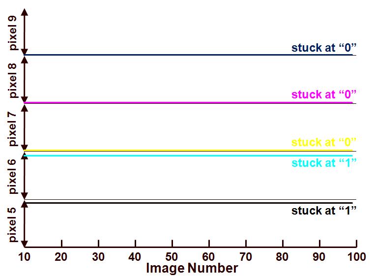
The result of this exercise is shown in the Figure 1 (the images used for this measurement is different from the data used in previous blogs).

Figure 1 : Behaviour of a first group of five dead pixels as a function of time.

The test images are taken with an exposure time of 20 ms.  On the horizontal axis the number of the image grabbed is shown (this can be seen as a time axis), and on the vertical axis the value of 5 dead pixels is shown.  (The pixel with the lowest number shows the lowest temporal noise.)  All five pixels shown demonstrate a noise level almost equal to 0 DN because all five pixels are fully saturated.

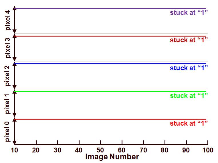
Another group of five pixels is shown in Figure 2.


Figure 2 : Behaviour of a second group of five dead pixels as a function of time.

In Figure 2, two more “white” pixels are shown, but also three “black” defects.  Although not visible in this graph, the temporal noise of the black pixels is not 0 DN, it still contains the noise of the output stage and the ADC.  This is not necessarily the case for the “white” defects, because they can be clipped by the ADC.

A final remark : this noise-based method to localize defect pixels cannot be used to find the “sick” pixels.  The latter ones are defined as pixels with a much larger or much smaller sensitivity than the average sensitivity of the sensor.  Because sick pixels still react to light, they can be found as being the outliers in the histogram of all pixels with light input.

Albert, 17-10-2012.

How To Measure RTS Pixels ?

October 4th, 2012

RTS stands for Random Telegraph Signal and is a very specific type of noise.  The pixels that do show RTS effects seem to switch between different (more or less) discrete states.  In most case they flip up and down between two signal levels.  This RTS effect can originate through :

–       dark current effects in the pixel itself, then the two flipping signal levels will be observed also as 2 RTS levels, or,

–       the effect of a single trap in the source follower, then the two flipping signal levels in combination with the CDS can be observed as 3 RTS levels, without CDS they remain as 2 RTS levels.

How can these RTS pixels be characterized or located ?  Actually the technique is very simple : because RTS pixels flip up and down between different states, they show a pretty large temporal noise.  So what can be done is the following :

–       grab several images (e.g. 100), with a relative long exposure time (100 ms or longer),

–       calculate on pixel level the temporal noise that the pixel demonstrates in the images grabbed,

–       rank all pixels according to the calculated noise, the pixels with the highest noise level come first and these are most probably RTS pixels,

–       track the value of these suspected RTS pixels over the frames grabbed.

The result of this exercise is shown in the Figure 1(the data used for this measurement is different from the data used in previous blogs).
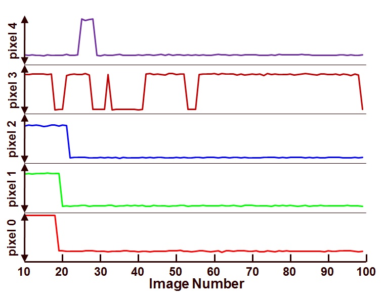
Figure 1 : Behaviour of a first group of five RTS as a function of time.

The images are taken with an exposure time of 2 s.  On the horizontal axis the number of the image grabbed is shown (this can be seen as a time axis), and on the vertical axis the value of 5 RTS pixels is shown.  (The pixel with the lowest number shows the largest temporal noise.)  Pixel 0, 1 and 2 change only once over the time of (90 x 2 s =) 3 min.  Pixel 3 is more lively and has several changes, notice that the time the pixel remains in the low state or the high state seems to be completely unpredictable.

Another group of five pixels is shown in Figure 2.

Figure 2 : Behaviour of a second group of five RTS as a function of time.

In Figure 2, pixel 5 is the one that attracts the attention : not only several transitions can be seen, but apparently the pixel switches between 3 states.  It is not immediately clear whether the third state is due to :

–       RTS of the dark current,

–       RTS of the source follower, or,

–       (most likely) due to a switching between two states somewhere half way the exposure time.

As can be learned, the RTS pixels can have very strange transition patterns, which are not predictable at all.  This leads to the challenge of calibrating these pixels during the manufacturing of the cameras.  In the case such a pixel behaves in the low state during calibration and in a high state during the application, the camera can show a white spot in the image captured …

Albert, 04-10-2012.
How To Measure “Photon Transfer Curve” (2) ?

September 19th, 2012

This blog will contain some further information on how to construct the Photon Transfer Curve, because it is possible to obtain the same information in various ways. What actually is needed for the PTC is a curve representing :

– the noise (standard deviation, variance, signal-to-noise ratio), versus,

– the sensor output signal (output signal, output signal corrected for offset or effective output signal), or,

– the sensor input signal (that was needed to generate the noise under consideration). Although none of the previous blogs did discuss this option, it is also a possible way to deduce the quantum efficiency by means of the PTC. This is the preferred way of using the PTC in the EMVA1288 standard. Unfortunately when measuring the input of the light level that goes to the sensor, one of the attractive features of the PTC is lost, being the fact that no absolute measurements of the light input is needed. For that reason here it is left out of the discussion.

To create a PTC curve the following options are available :

1) Grabbing images in dark : the dark current itself and the temporal noise measured in dark can be used to generate a PTC curve, although it would not be the first choice of doing ! But the dark current itself can be easily changed/modified and the noise can be very simply measured. Changing the dark current can be done by changing the exposure/integration time and/or by changing the temperature. Grabbing several images at the same setting (exposure time and temperature) can be used to calculate the temporal noise for each pixel. Averaging the obtained noise values and averaging the output signals can give rise to a single point on the PTC curve. Notice that more images and more pixels per image will lead to better results. In the case the noise distribution from pixel to pixel turns out to be too large, one can eliminate the outliers, or one can work with a smaller area instead of working with the complete sensor area. In principle the limited sensor area can be reduced to a single pixel, this is still enough to generate decent data for a PTC curve.

2) Grabbing images with uniform light input : the average output signal of a sensor under uniform illumination and the noise on pixel level can be easily calculated for a given integration time of the sensor. Also in this way a single point on the PTC curve can be obtained. It should be noted that the PTC curve is used to evaluate temporal noise and not non-uniformities of the light source. So special attention needs to be paid to the uniformity and stability of the light source. If a uniform light input over the total area of the sensor cannot be guaranteed, a reduced sensor area can be used to generate a PTC curve. In the extreme, one single pixel can be used to create the PTC curve.

3) Grabbing images with non-uniform light input : from the previous it can be learned that a single pixel can deliver the data for a PTC if the light intensity to this pixel is changed. On the opposite, if the light intensity across the various pixels of a sensor is changed, then each individual pixel can generate a particular point on the PTC curve. If one takes care that these pixels get a large variety of light input, then a complete PTC curve can be obtained. For example by means of :

a. Two sets of images, a first set with non-uniform light input and a second set with no light input. The second set is needed to generate a decent dark reference frame used to cancel the offset of every pixel. The first set is needed to generate the average signal as well as the temporal noise figure for every single pixel. It should be clear that the more images one gets in each set of images, the higher the accuracy will be of the PTC curve.

b. One set of images with a non-uniform light input and a single image in dark. In this case the single dark image can be used to compensate for the offset, but one should take into account that this dark frame is not noise free. Also in this case, a higher number of images in the first set will increase the accuracy of the PTC curve.

c. One set of images with a non-uniform light input. These are used to calculate the average output level and the temporal noise level of each pixel. In the case no dark reference frame is available, one can rely on the darkest area in the average output frame to define the offset. Although only an “educated” guess can be made of the offset, the accuracy of the PTC curve and the obtained results can be increased by grabbing as many as possible images.

In the training developed by Harvest Imaging, the construction of a Photon Transfer Curve gets a lot of attention.  It is amazing how low the number of input images/data needs to be to create a valuable evaluation tool for the camera or sensor.  For more information and exploration of the PTC method, you should attend one of the Harvest Imaging courses and say “Thank You” to Jim Janesick, who originally developed this technique.

Albert, 19-09-2012.