Incredible to belief that another year has passed by. Everything is moving so quickly, at least for us who are living in peace. Other people are facing other times. “The world is turning, I hope it will not turn away” (Uncle Neil in On The Beach).
In the beginning of 2024 I said goodbye to the Delft University of Technology. After 21 years of part-time working at TUD, my academic career came to an end. We celebrated that with a 1-day technical symposium. I absolutely enjoyed this farewell “party” very, very much. I could never ever dreamed of a better way to say goodbye to TUD. Many thanks again to the speakers, to the people who attended and to the TUD who supported me in the organization.
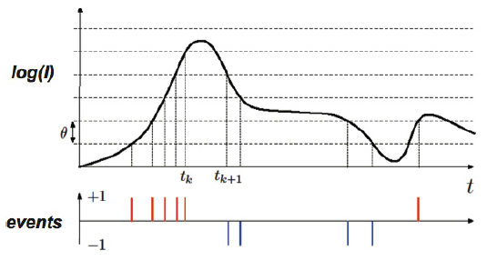
Another milestone in 2024 was the organization of the Harvest Imaging Forum around the topic “AI and VISION”. After a couple of times running the forum in a hybrid mode, I decided to run it only as an in-person event. The extra cost of hiring the A/V guys to broadcast the forum is really too high to make a break-even based on only the on-line registrations. Moreover, it turned out that a few people did not play the game as I expected they were going to do. In 2023 at least 2 persons (from different organizations) registered as single persons for the on-line event but had 20 people (or more) sitting in front of a huge screen to listen and watch the presentations. So I had to decide to abstain from live broadcasting or on-demand options of the forum. But that’s how it works : you have to learn from experience, also negative ones. For the coming year, the 11th forum will be organized. A few days ago I came to an agreement with the speaker as well as with the hotel. More info will follow some around coming Summer time.
What about 2025 ? Harvest Imaging will still continue with trainings. In 2025 several trainings are scheduled again, although only a very few “open” courses. As was the case in 2024, also in 2025 many in-house trainings are planned. (Don’t take in-house too literally, several of them have mixed groups from around the world, and in that case the courses run on-line). In the mean time, it became already a tradition : the Masterclass I run for Smithers (UK). In 2025 for the 5th year in a row I will present “The Latest Developments in the CIS World” during an on-line Masterclass (3 hours), scheduled in the beginning of March. This Masterclass is always quite a bit of preparation work : I do need about 90 … 100 sheets of brand new material, otherwise it does not comply with the title of Masterclass. “Recent Developments” covers the news of the last 12 months. Although it is a lot of work, it is fun to do. Keep in mind : “Teaching is learning twice !”
Finally, it is a pleasure for me to wish all my customers and readers a great Christmas and End Of The Year Season. Hopefully we see each other again in 2025, alive and kicking !
Albert.