BUTTING versus STITCHING (3)

August 9th, 2016

The stitching story started in the previous blog is not yet complete.  Further explanation deals with one-dimensional versus two-dimensional stitching, and single reticle versus multiple reticle stitching.

The difference between one-dimensional and two-dimensional stitching is straight forward.  If the stitching is done in one direction (vertical OR horizontal), it is known as one-dimensional stitching, if the stitching is done in two directions (vertical AND horizontal), it is known as two-dimensional stitching.  It should be clear that two-dimensional stitching gives the designer much more freedom in his/her design task, and does allow any device size to be designed.  Most of today’s lithographic equipment is capable of handling two-dimensional stitching, but in the earlier days, some type of alignment machines did allow only one-dimensional stitching.  For image sensors, the very first one-dimensional stitching was done by E2V, while the very first two-dimensional stitching was realized by Philips Research Labs.

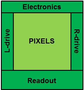
Another important discussion is the restriction to single reticle stitching or the option for multiple reticle stitching.  If the field of view of the lithographic machine is limited, it should be clear that (to limit the amount of stitchlines in the active imaging area) the full reticle size should be devoted to an array of pixels.  Consequently all peripheral parts and blocks need to be put on a second reticle.  This design strategy is known as multiple reticle stitching.  Unfortunately most fabs are not so happy with multiple reticle stitching because the reticles have to be exchanged during the exposure of the wafers.  This is time consuming, puts a burden on the use of the equipment and is costing a lot of extra money.  For that reason most fabs (if they offer stitching at all) prefer single reticle stitching.  Another important factor to avoid multiple reticle stitching is the cost of the extra mask set.  For more advanced CMOS processes, the mask cost is not negligible anymore compared to the cost of the wafer processing.  It was Philips Research Labs that fabricated for the first time large area imagers based on multiple reticle stitching.

As a consequence, single reticle stitching is much more common than multiple reticle stitching.  In that case, the active imaging array together with the peripheral blocks need to fit on a single reticle size, which leaves a smaller area for the pixel array (compared to a full reticle size in the case of multiple reticle stitching).  Resulting in more exposures for the active area, more stitch lines, more processing time and more expensive processing.  On the other hand, one needs only one mask set.

Altogether in the case of large-area imagers, very often a designer likes to go for multiple reticle, two-dimensional stitching (to avoid too many stitch lines), while most fabs prefer to avoid stitching at all.  It is not always an easy exercise to find an optimum between these two extremes.  There are only a very limited number of fabs/foundries in the world that do allow their customers to go for two-dimensional, multiple reticle stitching.  If stitching is offered at all, then the most common option is single reticle stitching in combination with one-dimensional stitching.

Albert, 09-08-2016.

BUTTING versus STITCHING (2)

July 8th, 2016

After the butting, it is now stitching time !

To explain the stitching, Figure 1 is included that shows the complete top-level design/lay-out of an image sensor (CCD or CMOS).


Figure 1 : Sketch of the top-level design of an image sensor.

One can recognize the following parts :

  • The pixel matrix, consisting of r by s pixels,
  • The left (L-) driving and right (R-) driving electronics,
  • Some extra electronics at the top (e.g. biasing circuitry, etc.),
  • The readout part (consisting for instance of CDS, PGA, ADC and other beautiful stuff),
  • And 4 blocks at the corner, they can contain timing generation, reference generation, maybe ADCs if they are not implemented on the columns, etc.

During the normal design phase, one or more designers take care about all these separate blocks and at the end of the design process, all blocks are nicely put together, the design is checked and finally the complete lay-out is sent to the mask shop to fabricate the masks.  Such a mask set normally consists of several reticles/masks, and in most cases, every layer of the lay-out (active area, implants, poly-layer, contact openings, vias, metal layers, etc.) is put on a separate reticle/mask.  As an example, a “simple” CMOS imaging process consists of 30 reticles (or more).  The maximum useful area of a reticle, defined by the field of view of the lithographic equipment, is about 25 mm x 25 mm (the numbers given here are indications and differ from machine to machine).

The limitation of the reticle area is defining the maximum size of the chip, unless stitching is applied.  Stitching is a technology that allows the designer to fabricate an image sensor that is larger than the field of view of the lithographic equipment, still making use of reticles that fit into the field of view of that equipment.  Moreover, the size of the sensor will only be limited by the wafer size (and the budget of the customer).

To realize a sensor larger than the reticle size, the following strategy is applied : the very last stage in the design, being putting together the major building blocks as shown in Figure 1, is omitted.  The building blocks themselves are put on the reticle as individual pieces of the design.  This concept is shown in Figure 2.

Figure 2 : Isolated building blocks put separately on the reticle.

These building blocks cannot be used as separate circuits, they can only operate in connection with each other.  By appropriate programming the lithographic tool, each individual block of the reticle can be selected (by means of mechanical blading) and can be transferred into the photoresist on the wafer.  In this way it is possible to “stitch” the various blocks together on the wafer during the lithographic process.  But because the blocks are stitched during the wafer manufacturing process, it is also possible to make other configurations (than the one shown in Figure 1) by means of multiple use of the various blocks.  An example is illustrated in Figure 3, where the matrix of pixels is repeated 6 times.  To complete the sensor, several other blocks need to be repeated twice or threefold as well.  And in this way, an image sensor can be fabricated that is larger than the field of view of the reticle.


Figure 3 : Extending the size of the sensor beyond the reticle field of view.

If the design of the various blocks is carefully done to avoid stitching artifacts, then actually the final device shown in Figure 3, will look like the one illustrated in Figure 4.  The stitch lines will no longer be visible or noticeable, and the end result of the stitching technology is a large-size, monolithic image sensor.


Figure 4 : Final imaging array after stitching.

These days, stitching is widely applied in the digital imaging industry.  Various lithographic tools have different sizes of the reticle field of view, but in general terms, one can state that all full-format imagers (36 mm x 24 mm) or larger are stitched devices.

Albert, 08-07-2016.

Harvest Imaging Forum 2016 : update

June 21st, 2016

Registration is open since a couple of weeks for two sessions in December 2016, see www.harvestimaging.com/forum_introduction_2016.php

For those interested to attend, make sure you register a.s.a.p. for one of the two sessions, because this time there will be NO third session.

The Harvest Imaging Forum 2016 will be limited to maximum two sessions that each have a limited amount of seats.

Albert, 21-06-2016.

BUTTING versus STITCHING (1)

June 17th, 2016

Although most imaging engineers are aware about both technologies of butting and stitching, still some question marks exist about what is what ?  This blog as well as the next one try to give some answers to this question.

Butting is referring to tiling closely together separate pieces of silicon to come to one large sensitive array.  In principle all separate pieces of silicon can be operated as a single image sensor.  In most cases butting is used to make imagers that are larger than the largest imager a single wafer can hold.

Stitching is referring to putting various design blocks together during the processing of the silicon, to make one large, stand-alone imaging array.  All separate blocks of the design cannot be operated as a single image sensor, neither are they available as isolated dies.  In most cases stitching is used to make imagers that are larger than the field of view of the lithographic equipment used during the fabrication of the imagers.

Are all buttable devices also stitched ?  Most of them are, because in many cases stitching is needed to make the largest array possible on a single wafer.  If that imager is still not large enough, butting is the only solution.

Are all stitched devices also buttable ?  For sure not, because not all stitched devices have a wafer-level size.

In Figure 1 a simple sketch is shown of an imaging array : the pixel matrix is surrounded by a left-driving and right driving circuitry, a readout part at the bottom and some extra electronic circuitry at the top.


Figure 1 : Sketch of the floor plan of an image sensor.

This sensor is not designed to be butted, because the circuitry around the imaging matrix is preventing a contiguous larger imaging area when two or more devices are placed next to each other.  To make this device buttable, at the circuitry along at least one side needs to be removed in the design.  An example is shown in Figure 2, with the result after butting in Figure 3.

Figure 2 : One-side buttable imaging array.

Figure 3 : Two devices butted together based on the device concept of Figure 2.

As can be seen in Figure 3, the total light sensitive array is twice as large as the size of a single device.  Butting will never ever be perfect in the sense that there will always some pixels missing between the two pieces of silicon.  But in most applications, the number of lines (in Figure 3) of missing pixels is limited to a single line of pixels.  It has to be mentioned that devices that are butted normally do not use small pixels.  But pixel sizes of several tens of micro-meters are very common for buttable devices.

The limitation of the sketch in Figure 3 is clear : only a factor of 2 ins ensitive area can be gained by butting 2 devices.  If a larger sensitive area is needed, buttability needs to be possible along more than 1 side, for instance 2 sides, as shown in Figure 4.

Figure 4 : Two-sides buttable imaging array.

Figure 5 : Four devices butted together based on the device concept of Figure 4.

The same accuracy as mentioned before can be obtained along the butting lines : only one column or one row of pixels will be missing.  Notice the rotated arrangement of the dies in Figure 5.  From bottom left to bottom right, rows are becoming columns and columns are becoming rows, etc.  So a little extra data reshuffling is needed after readout, but after all, a factor of 4 can be gained in light sensitive area compared to a single die shown in Figure 4.

A buttable configuration with more flexibility can be found with devices that are 3-sides buttable, shown in Figure 6.


Figure 6 : Three-sides buttable imaging array.

All electronics needed to drive the sensor is no longer available at the sides, neither at the top of the chip.  But the drivers and timing circuitry is placed between the pixels themselves.  The lay-out of the chip is becoming more and more sophisticated, because as can be seen in Figure 7, butting does not allow any circuitry at the butting edges.

Figure 7 : Six devices butted together based on the device concept of Figure 6.

But the big advantage of this design is the unlimited butting capability in one direction.  Of course in the other direction the number of devices is limited to 2.

The latter architecture is widely used for medical (mainly CMOS) and astronomy (mainly CCD, slow shift towards CMOS) applications.  With today’s 300 mm wafer sizes, single monolithic sensors of 200 mm x 200 mm on a single wafer can be made.  And with the butting x mm (H) x 400 mm (V) are possible, where x is defined by the application and the cost of the assembled device. (With a rectangular footprint of the sensor instead of a square one, even larger butted imaging arrays are possible.)

What about 4 sides buttable ?  To my knowledge a 4-sides buttable device is never realized in CMOS technology, although there were some attempts in the past to build 4-sides buttable CCDs.  But the wiring and the connections to the outside world are becoming extremely complex and difficult.  And with the existence of 300 mm wafers, there is much less justification left to design and fabricate 4-sides buttable devices (maybe with the exception of astronomy applications).

Next time the focus will be on stitching,

Albert, 17-06-2016

Difference between binning and averaging (2)

June 3rd, 2016

In the previous blog the focus was on binning (charge, voltage and digital domain) in the case the readout noise was dominating over the photon-shot noise.  In other words, for the case of small signals or low light levels.  This time, the situation for a shot-noise limited condition is considered.  And actually the story can be very short : it does not matter when or where the binning is done, in all cases the result is exactly the same.

For the charge domain : if n x n charge packets are added together, each with m electrons, then after binning the final charge packet holds :

n x n x m electrons.

The photon-shot noise in each individual charge packet was

sqrt(m) electrons,

so the SNR for every individual charge packet was

SNR = m/sqrt(m) = sqrt(m).

After binning the total photon-shot noise is equal to

sqrt(n x n x m) electrons

and the SNR will be equal to :

SNR = n x n x m/sqrt(n x n x m) = sqrt (n x n x m).

After binning in the charge domain, the increase in SNR will be

sqrt(n x n x m)/sqrt(m) = n !

For the voltage domain or digital domain : if n x n signals are added together, each with m electrons, then before binning the output signal would have been k x m V or DN, with k being the conversion gain from input (charge) to output (Volts or Digital Numbers).  Then after binning the final signal will be

n x n x k x m V or DN.

The photon-shot noise of each individual signal before binning was

k x sqrt(m) V or DN,

so the SNR for the individual signal before binning was

SNR = (k x m)/(k x sqrt(m)) = sqrt(m).

After binning the total photon-shot noise is equal to

k x sqrt(n x n x m)

and the SNR will be equal to :

SNR = (n x n x k x m)/(k x sqrt(n x n x m)) = sqrt (n x n x m).

After binning in the voltage of digital domain, the increase in SNR will be

sqrt(n x n x m)/sqrt(m) = n !

Conclusion : if there is enough light so that the performance of the sensor or the camera is shot-noise limited, it does not matter how the binning is realized, charge domain, voltage domain or digital domain.  The increase of the SNR after binning is always equal to a factor n, being the kernel size in the case of n x n binned pixels.

Albert, 31-05-2016.

HARVEST IMAGING FORUM 2016 “Robustness of CMOS Technology and Circuitry”

May 29th, 2016

I am happy to inform you that the registration for the 2016 Harvest Imaging Forum is open !

Visit the web-pages of the forum at www.harvestimaging.com/forum_introduction_2016.php

Best wishes, Albert.

29-05-2016.

Difference between binning and averaging (1)

May 21st, 2016

Especially in the CMOS world there seems to be some confusing about the definition of binning and averaging.

Binning is a technique that allows to add up two (or more) pixel output signals to increase the signal-to-noise ratio of the image sensor at the expense of resolution.  The original binning method was done by means of adding of the output signals in the charge domain, but with the introduction of CMOS imagers, binning is also applied in the voltage domain or digital domain.  The charge domain binning is always done on-chip, voltage binning or digital binning can be done on-chip as well as off-chip.

Charge domain binning : this is the only binning method that can be completely done noiseless.  In the case n pixels are binned, the signal after binning will be n times the signal of each individual pixel.  Readout of the signal after binning will only once add the noise of all readout circuitry (= readout noise), so the signal-to-noise ratio AFTER binning is equal to n times the signal-to-noise ratio of the un-binned signal.

Charge domain binning is very easy to implement in monochrome CCDs by means of an adapted timing, colour CCDs may need a more complicated clocking scheme and/or a dedicated design to perform binning because charge domain binning needs to be done in each colour plane.  Charge domain binning in CMOS image sensors is limited to pixels that share a floating diffusion.

Voltage or digital domain binning : both binning methods can only be applied AFTER the pixels are being readout, and thus after the readout noise is included in the output signal.  In the case n pixels are binned, the signal after binning will be n times the signal of each individual pixel, but the noise will be added in quadrature, and will be equal to ?n times the noise of a single pixel.  So the signal-to-noise ratio after binning in the voltage or digital domain will be ?n times the original signal-to-noise ratio.

Averaging of signals takes place when two (or more) capacitors holding pixel output signals in the voltage domain are short-circuited.  The charges on each capacitor are summed, but so are the capacitances.  In the simple case of averaging n signals (present on n capacitors of equal value), the averaged signal will not change in value.  But the noise on the other hand will be added in quadrature and will be stored on the summed capacitors.  Any idea what will happen with the final signal-to-noise ratio ?

Conclusion : charge domain binning is more efficient in increasing the signal-to-noise ratio compared to binning/averaging in the voltage domain or binning in the digital domain.  The explanation of binning and averaging as well as the discussion about signal-to-noise ratio in this blog takes into account that the noise content of the pixel output signals is dominated by readout noise.  The story becomes slightly different is the signals are shot-noise limited.  This will be explained next time.

Albert, 21-05-2016.

Update of the Phase-Detection Auto-Focus Pixel Report

April 19th, 2016

A new update of the PDAF report is available.  Compared to the previous version, extra information is included about a figure-of-merit.  This FoM allows the reader to compare the efficiency of the PDAF pixels coming from different sensors, different technologies and different vendors.  Also a couple of new references are added to list.

If you are interested in buying (unfortunately it is not free of charge) the PDAF report, including the two updates, please contact me through info (at) harvestimaging (dot) com.

Thanks a lot, Albert.

19 April 2016.

Announcement of the fourth Harvest Imaging Forum in December 2016

April 17th, 2016

Mark now already your agenda for the fourth Harvest Imaging Forum, scheduled for December 2016.

After the succesful gatherings in 2013, 2014 and 2015, I am happy to announce a fourth one.  Also this fourth Harvest Imaging Forum will be a high-level, technical, short course focusing on one particular hot topic in the field of solid-state imaging.  The audience will be strictly limited, just to stimulate as much as possible the interaction between the participants and speaker(s).

The subject of the fourth forum will be :

“Durability of CMOS Technology and Circuitry outside the Imaging Core : integrity, variability and reliability”.

More information about the speaker and the agenda of the fourth forum will follow in the coming weeks, but I wanted to share this announcement with you as early as possible to make sure you can keep your agenda free on these days (Dec. 9-10 or Dec. 12-13, 2016).

Albert,

April 17th, 2016.

Imaging Trainings scheduled for Spring 2016

February 27th, 2016

Maybe it is good to remind the visitors of this blog about imaging trainings in the Spring 2016.  There are 6 courses in the pipeline :

– a 2-day class to get an introduction in the world of CMOS image sensors.  This class is intended for people who have almost no background in solid-state imaging.  This course takes place in Taufkirchen (Munich) on June 29-30, 2016, organization through www.framos.com.

– a 5-day class if you want to learn more about imagers than just the working principles.  Also this class is intended for “new-comers” in the field, but also people working already a few years in imaging can revitalize their knowledge.  The course can be considered as the mother of all trainings offered by Harvest Imaging.  Key to this class are the exercise sessions at the end of every day helping the participants to put the theory into practice.   This course takes place on April 4-8, 2016 in Barcelona, and is organized by www.cei.se.

– a 2-day class with hands-on measurements and evaluation of an “unknown” camera.  Because the participants have to perform all characterization work themselves, this course is NOT intended for people fresh in the imaging field.  Preferably the course participants have a few years of experience in the arena of solid-state imaging.  This course takes place in Munich, on March 30-31, 2016, organized by www.framos.com, as well as in Amersfoort, on May 26-27, 2016, organized by www.cei.se.

– a 3-day advanced class focusing on CMOS image sensors.  Because the material presented is on a higher level, this course is intended for people who have a couple of years of experience in the field of digital imaging.  The course is scheduled for May 23-25, 2016 in Amersfoort (Nl), organized by www.cei.se.

– a 3-day course on Digital Camera Systems.  In this training the focus is less on the image sensors, but more on the processing of the signal delivered by the image sensor.   The complete colour processing pipe will be explained and demonstrated by an extensive amount of images and algorithms.  The participants will get a soft copy of all images shown in the course.  Location will be Barcelona, date : June 14-16, organized by www.cei.se.

Looking forward to see you at one of these courses.

Albert, 27 February 2016