After the butting, it is now stitching time !
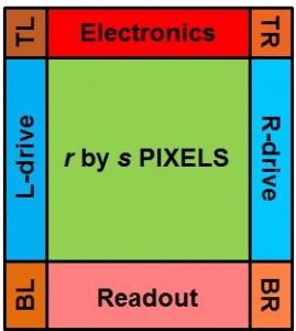
To explain the stitching, Figure 1 is included that shows the complete top-level design/lay-out of an image sensor (CCD or CMOS).
Figure 1 : Sketch of the top-level design of an image sensor.
One can recognize the following parts :
- The pixel matrix, consisting of r by s pixels,
- The left (L-) driving and right (R-) driving electronics,
- Some extra electronics at the top (e.g. biasing circuitry, etc.),
- The readout part (consisting for instance of CDS, PGA, ADC and other beautiful stuff),
- And 4 blocks at the corner, they can contain timing generation, reference generation, maybe ADCs if they are not implemented on the columns, etc.
During the normal design phase, one or more designers take care about all these separate blocks and at the end of the design process, all blocks are nicely put together, the design is checked and finally the complete lay-out is sent to the mask shop to fabricate the masks. Such a mask set normally consists of several reticles/masks, and in most cases, every layer of the lay-out (active area, implants, poly-layer, contact openings, vias, metal layers, etc.) is put on a separate reticle/mask. As an example, a “simple” CMOS imaging process consists of 30 reticles (or more). The maximum useful area of a reticle, defined by the field of view of the lithographic equipment, is about 25 mm x 25 mm (the numbers given here are indications and differ from machine to machine).
The limitation of the reticle area is defining the maximum size of the chip, unless stitching is applied. Stitching is a technology that allows the designer to fabricate an image sensor that is larger than the field of view of the lithographic equipment, still making use of reticles that fit into the field of view of that equipment. Moreover, the size of the sensor will only be limited by the wafer size (and the budget of the customer).
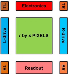
To realize a sensor larger than the reticle size, the following strategy is applied : the very last stage in the design, being putting together the major building blocks as shown in Figure 1, is omitted. The building blocks themselves are put on the reticle as individual pieces of the design. This concept is shown in Figure 2.
Figure 2 : Isolated building blocks put separately on the reticle.
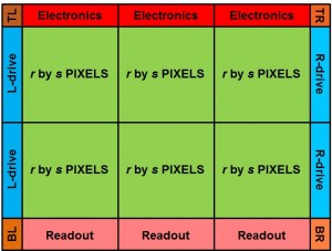
These building blocks cannot be used as separate circuits, they can only operate in connection with each other. By appropriate programming the lithographic tool, each individual block of the reticle can be selected (by means of mechanical blading) and can be transferred into the photoresist on the wafer. In this way it is possible to “stitch” the various blocks together on the wafer during the lithographic process. But because the blocks are stitched during the wafer manufacturing process, it is also possible to make other configurations (than the one shown in Figure 1) by means of multiple use of the various blocks. An example is illustrated in Figure 3, where the matrix of pixels is repeated 6 times. To complete the sensor, several other blocks need to be repeated twice or threefold as well. And in this way, an image sensor can be fabricated that is larger than the field of view of the reticle.
Figure 3 : Extending the size of the sensor beyond the reticle field of view.
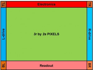
If the design of the various blocks is carefully done to avoid stitching artifacts, then actually the final device shown in Figure 3, will look like the one illustrated in Figure 4. The stitch lines will no longer be visible or noticeable, and the end result of the stitching technology is a large-size, monolithic image sensor.
Figure 4 : Final imaging array after stitching.
These days, stitching is widely applied in the digital imaging industry. Various lithographic tools have different sizes of the reticle field of view, but in general terms, one can state that all full-format imagers (36 mm x 24 mm) or larger are stitched devices.
Albert, 08-07-2016.


